
Bombardment with tightly focused electron beams has been suggested as a means of electrically disabling selected individual carbon-nanotubes (CNTs) in electronic devices. Evidence in support of the suggestion was obtained in an experiment in which a CNT field-effect transistor was disabled (see figure) by focusing a 1-keV electron beam on a CNT that served as the active channel of a field-effect transistor (FET).
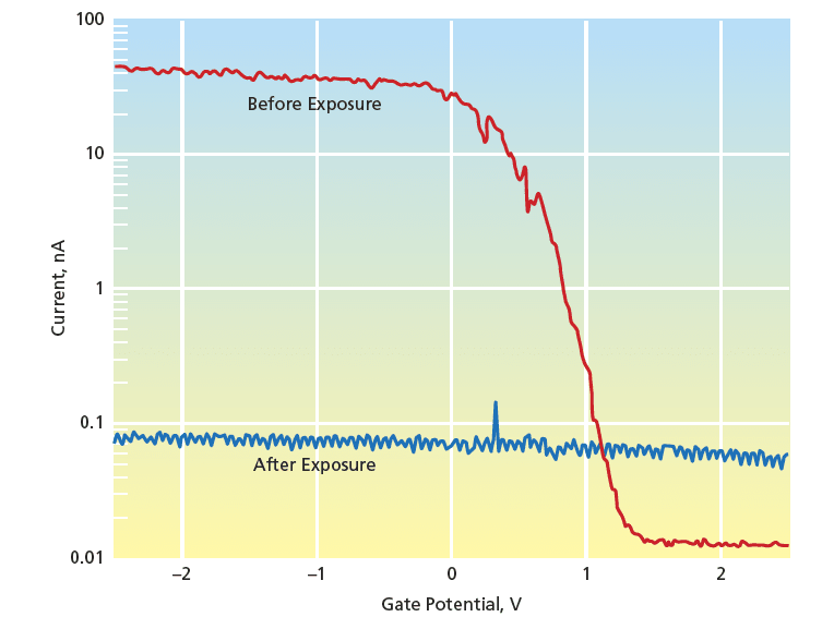
According to the suggestion, by using a 1-keV electron beam (e.g., a beam from a scanning electron microscope), a particular nanotube could be rendered electrically dysfunctional. This procedure could be repeated as many times as necessary on different CNTs in a device until all of the excess CNTs in the device had been disabled, leaving only one CNT as an active element (e.g., as FET channel).
The physical mechanism through which a CNT becomes electrically disabled is not yet understood. On one hand, data in the literature show that electron kinetic energy >86 keV is needed to cause displacement damage in a CNT. On the other hand, inasmuch as a 1-keV beam focused on a small spot (typically a few tens of nanometers wide) deposits a significant amount of energy in a small volume, the energy density may suffice to thermally induce structural and/or electronic changes that disable the CNT. Research may be warranted to investigate this effect in detail.
This work was done by Mihail Petkov of Caltech for NASA's Jet Propulsion Laboratory.
This Brief includes a Technical Support Package (TSP).
Disabling CNT Electronic Devices by Use of Electron Beams
(reference NPO-41343) is currently available for download from the TSP library.
Don't have an account?
Overview
The document titled "Disabling CNT Electronic Devices by Use of Electron Beams" is a Technical Support Package from NASA's Jet Propulsion Laboratory (JPL), focusing on the challenges and solutions related to carbon nanotubes (CNTs) in electronic devices. CNTs are recognized for their exceptional electronic properties, making them ideal candidates for applications in non-volatile memory and field-effect transistors (FETs). However, a significant challenge in utilizing CNTs is the inability to grow them at specific locations and orientations, leading to devices with inconsistent electronic characteristics due to the statistical distribution of CNTs.
The document outlines a novel solution to this problem: the use of a 1 keV electron beam to disable excess CNTs in a device. By focusing the electron beam on a specific CNT, it is possible to render it dysfunctional, thereby allowing only one CNT to remain active as the channel in a FET. This method addresses the issue of having multiple CNTs, which can lead to varied switching voltages and gains, ultimately affecting device performance.
The document also discusses the underlying physics of this approach. While literature indicates that higher energy levels (over 86 keV) are required to cause displacement damage in CNTs, the focused 1 keV beam can deposit significant energy into a small volume, potentially inducing structural or electronic changes that disable the CNT. This innovative technique opens up new avenues for research and development in CNT technology, particularly in enhancing the reliability and performance of electronic devices.
Additionally, the document serves as a resource under NASA's Commercial Technology Program, aiming to disseminate aerospace-related developments with broader technological and commercial applications. It provides contact information for further inquiries, emphasizing the collaborative nature of this research and its potential impact on various industries.
In summary, this Technical Support Package presents a significant advancement in CNT technology, offering a practical solution to a critical challenge in electronic device fabrication. The use of electron beams to selectively disable CNTs could lead to improved performance and reliability in future electronic applications, showcasing the innovative spirit of NASA's research initiatives.