
Metal emitter structures in a class of developmental InP-based high-speed heterojunction bipolar transistors (HBTs) have been redesigned to have Tshaped cross sections. More precisely, the modified cross sections can be characterized as having highly stylized T-shapes that are modified versions of prior trapezoidal shapes (see figure). T- cross- section metal features have been widely used in Schottky diodes and high electron- mobility transistors, but not in HBTs. As explained below, the purpose served by the present T- cross-sectional shapes is to increase fabrication yields beyond those achievable with the prior cross-sectional shapes.
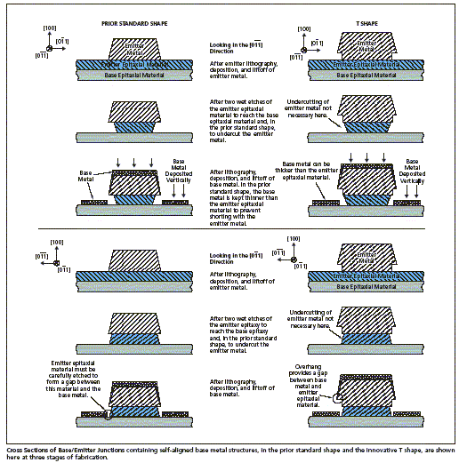 At the beginning of the program to develop these HBTs, some of the HBTs were fabricated to contain self-aligned base metal structures and some to contain non-self-aligned base metal structures. For the ones containing self- aligned base metal structures, fabrication lots exhibited low yields and high degrees of nonuniformity, which were attributable to inadequate definition of base/emitter junctions. Yields were reduced by the need to reject transistors that had leaky junctions. One of the primary causes of leakage at the junctions was short- circuiting of the base metal to emitter semiconductor epitaxial material that had not been sufficiently removed from the vicinity of the base metal during the wet-etch undercut procedure. The existence of this cause was observed in some cases from scanning electron microscopy and indirectly deduced from the observation that the yields of HBTs containing non- self- aligned base metal structures were more than double the yields of HBTs containing self-aligned base metal structures.
The incidence of leakage is smaller in the non- self- aligned case because the base metal is spaced farther from the emitter at the outset. In contrast, in the self- aligned case, the base metal is separated from the emitter epitaxial material by only the amount of the emitter undercut effected in the aforementioned etching. Self- aligned base metal structures are preferred over non- self- aligned ones because the resulting base resistances are smaller, leading to better transistor performances.
The T-shaped cross section reducesthe likelihood of short-circuiting of base metal to epitaxial emitter material, thereby helping to increase fabrication yield, in the following way: The overhang portion of the T acts as an awning- like deposition mask. The base metal is deposited predominantly unidirectionally (vertically downward in the figure) by evaporation, and deposition is prevented or reduced in the shadow area that lies under the overhang and adjacent to the emitter epitaxial material.
The T- shape also offers other benefits:
- Requirements for controlling undercut etching are relaxed; as a consequence, emitter/base definition processes are simplified.
- The relaxation of requirements makes it possible to use thicker base metal deposits, thereby reducing the inductances and the electrical and thermal resistances of base metal structures.
This work was done by King Man Fung, Lorene Samoska, James Velebir, Richard Muller, Pierre Echternach, and Peter Siegel of Caltech; Peter Smith of Cree, Inc.; Suzanne Martin of Wavestream Corp.; Roger Malik of RJM Semiconductor; and Mark Rodwell, Miguel Urteaga, Vamsi Paidi, and Zack Griffith of UC Santa Barbara for NASA's Jet Propulsion Laboratory. For further information, access the Technical Support Package (TSP) free on-line at www.techbriefs.com/tsp under the Electronics/Computers category. NPO-41034
This Brief includes a Technical Support Package (TSP).
T-Shaped Emitter Metal Structures for HBTs
(reference NPO-41034) is currently available for download from the TSP library.
Don't have an account?
Overview
The document is a Technical Support Package from NASA's Jet Propulsion Laboratory (JPL) detailing advancements in the fabrication of Heterojunction Bipolar Transistors (HBTs) utilizing T-shaped emitter metal structures. It addresses the challenges associated with the standard fabrication process, particularly the self-aligned base-emitter junction, which typically involves a wet etch that undercuts the emitter metal stripe. This process has been found to be difficult to control, leading to inconsistent undercutting and malfunctioning base-emitter junctions due to shorting between the base metal and the emitter epitaxy.
The report emphasizes the importance of the T-emitter metal spacer, which is crucial for preventing linearly evaporated metal from shorting to the emitter epitaxial layer. The document includes specific technical details, such as the dimensions of the T-emitter metal HBT, which has an emitter area of 2x0.6x4 μm², and the operational parameters, including an emitter current density (Je) of 190 kA/cm² and a collector-emitter voltage (Vce) of 3V. The performance metrics of the device are highlighted, with an extrapolated current gain cutoff frequency (Ft) of 142 GHz and a power gain cutoff frequency (Fmax) of 160 GHz.
Figures included in the document illustrate the fabrication process and the structure of the T-emitter, providing visual context to the technical descriptions. The report also notes that the findings are part of a broader effort to enhance the reliability and performance of HBTs, which are critical components in various electronic applications, particularly in high-frequency and high-power environments.
Additionally, the document serves as a resource for those interested in aerospace-related developments with potential applications in other technological fields. It encourages further exploration of the research and technology in this area, directing readers to the NASA Scientific and Technical Information (STI) Program Office for additional resources.
Overall, this Technical Support Package encapsulates significant advancements in HBT technology, addressing fabrication challenges and presenting solutions that enhance device performance, thereby contributing to the ongoing evolution of semiconductor technology in aerospace and beyond.