
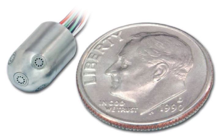
This work focused on developing, fabricating, and fully calibrating a flow-angle probe for aeronautics research by utilizing the latest microelectromechanical systems (MEMS), leadless silicon on insulator (SOI) sensor technology. While the concept of angle probes is not new, traditional devices had been relatively large due to fabrication constraints; often too large to resolve flow structures necessary for modern aeropropulsion measurements such as inlet flow distortions and vortices, secondary flows, etc. Measurements of this kind demanded a new approach to probe design to achieve sizes on the order of 0.1 in. (≈3 mm) diameter or smaller, and capable of meeting demanding requirements for accuracy and ruggedness.
The proposed device is capable of providing flow measurements for highfrequency, small-flow structures, and broad flow-field coverage as necessary for subsonic diffuser and exhaust nozzle flows. This design eliminates packaging redundancy by directly mounting SOI sensor components onto the flow angle probe body. The five-hole probe design achieved the following characteristics:
• Small size: The small size allows detailed flow structure data such as flow distortions due to shock boundary interaction, crosswind effect, and inlet vortices, and better matches the characteristic frequencies associated with the probe size (due to vortex shedding, for example) with the inherent high-frequency response of the sensors (over 100 kHz). Further, the minimal frontal area will allow multiple sensor rakes to be fabricated for inlet flow field survey.
• High-frequency response above 50 kHz: This is achievable by mounting pressure-sensing elements directly onto the flow angle probe, thus avoiding plenum/cavity-related acoustic resonances.
• Measurement accuracy of 35° range: By utilizing computational dynamic tools as well as calibrated wind tunnel facilities, flow shape optimization and software reduction techniques shall be developed to support this objective.
• Multiple function: A single, compact probe designed to deliver two flow angles (pitch and yaw), as well as pressure and Mach information, allows complete flow field characterization in both space and time.
• High-temperature capability: All-welded design utilizing all high-temperature materials in the construction.
• Harsh environment operability: Leadless sensor technology hermetically protects the entire sensing network while completely eliminating all the wire bonds. Only the silicon (backside) of the sensor is exposed to the pressure media. The addition of screens in the high-temperature version allows for protection from particle impact.
This work was done by Alex Ned, Anthony Kurtz, Tonghuo Shang, and Scott Goodman of Kulite Semiconductor Products, Inc.; and Gerald Guenette of MIT for Glenn Research Center.
Inquiries concerning rights for the commercial use of this invention should be addressed to NASA Glenn Research Center, Innovative Partnerships Office, Attn: Steven Fedor, Mail Stop 4–8, 21000 Brookpark Road, Cleveland, Ohio 44135. Refer to LEW-18938-1.