
Microelectromechanical sensors based on magnetoresistance have been proposed. Like other microelectromechanical sensors, these would be used to measure physical quantities that can be made to manifest themselves in small mechanical displacements. Potential applications for microelectromechanical sensors include accelerometers, magnetometers, bolometers, pressure sensors, seismometers, Golay cells, and microphones. Potential markets include the aerospace, biomedical, semiconductor, automotive, and defense industries.
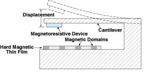
The proposed sensors are expected to be less problematic, because they would be manufactured and operated by use of techniques that have become well established in the data-storage (computer-disk) industry. In a typical sensor of proposed type, a magnetoresistive device mounted on a diaphragm or near the free end of a cantilever in a magnetic-field gradient (see figure) would be used to measure the field strength and thus, indirectly, the distance from the source of the magnetic field. This distance would, in turn, be indicative of the displacement of the diaphragm or cantilever from an equilibrium distance. The magnetic field would be provided by a hard magnetic thin film attached to the relatively stationary portion of the device structure, facing the magnetoresistive device. The strength and gradient of the magnetic field would depend partly on the thickness of the film and partly on the distances between magnetic domains in the film.
Unlike in a tunneling-based sensor, it would not be necessary to maintain a distance of about 1 nm or less between tunneling tips; instead, the film thickness and thus the magnetic-field strength could be increased to enable the use of a greater equilibrium distance between the magnetoresistive device and the film, making the proposed sensor less vulnerable to damage. Also, inasmuch as techniques for measuring magnetic fields are well established in the data-recording industry, magnetic-field changes corresponding to subnanometer displacements could be measured accurately.
This work was done by John D. Olivas and Bruce Lairson of Caltech for NASA's Jet Propulsion Laboratory. For further information, access the Technical Support Package (TSP) free on-line at www.nasatech.com/tsp under the Physical Sciences category.
This invention is owned by NASA, and a patent application has been filed. Inquiries concerning nonexclusive or exclusive license for its commercial development should be addressed to
the Patent Counsel
NASA Management Office–JPL; (818) 354-4770.
Refer to NPO-20146.
This Brief includes a Technical Support Package (TSP).
Microelectromechanical Sensors Based on Magnetoresistance
(reference NPO-20146) is currently available for download from the TSP library.
Don't have an account?
Overview
The document presents a report on a novel microelectromechanical sensor (MEMS) technology that utilizes magnetoresistance principles to measure small displacements in cantilevers or diaphragms. This innovation addresses significant limitations associated with traditional tunneling tip technology, which has been widely used in MEMS but suffers from issues related to tip spacing, reliability, and manufacturing challenges.
The report outlines the motivation behind developing this new sensor technology. Traditional MEMS that rely on tunneling tips require extremely precise spacing of about one nanometer, which is difficult to achieve and maintain. This precision leads to uncertainties in electrical behavior and potential damage during operation, resulting in high rejection rates of faulty parts. The new sensor design aims to eliminate these issues by employing a giant magnetoresistive (GMR) sensor to detect variations in magnetic field strength, which correlates with the movement of the cantilever or diaphragm.
The proposed solution leverages established thin film deposition techniques used in the data storage industry, which have already addressed many of the processing challenges faced in manufacturing. By using magnetic materials, the new sensors can maintain greater spacing than traditional designs, significantly reducing the risk of damage during fabrication. This approach allows for accurate measurements of nanometer and sub-nanometer displacements, enhancing the robustness and reliability of the sensors.
The document also includes a summary of test results, although specific data is not detailed in the provided excerpts. The acknowledgment section suggests that the work is supported by references and contributions from various individuals, indicating a collaborative effort in the development of this technology.
Overall, this MEMS technology represents a significant advancement in sensor design, promising improved performance and reliability for applications in various fields, including aerospace, biomedical, and automotive industries. The innovative use of magnetoresistance not only addresses the shortcomings of existing technologies but also opens new avenues for precise measurement and monitoring in micro-scale applications.