
Efforts are under way to develop deformable mirrors equipped with microscopic electrostatic actuators that would be used to maintain their reflective surfaces in precise shapes required for their intended applications. Unlike actuators that depend on properties of materials (e.g., piezoelectric and electrostrictive actuators), electrostatic actuators are effective over a wide temperature range. A mirror of the present type would be denoted a MEMS-DM (for microelectromechanical system deformable mirror). The reflective surface of such a mirror would be formed on a single-crystal silicon membrane that would be attached by posts to a silicon actuator membrane that would, in turn, be attached by posts to a rigid silicon base (see figure).
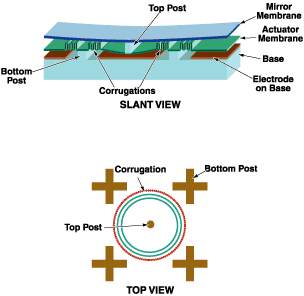
The mirror and actuator membranes and posts would be fabricated partly by surface and partly by bulk micromachining of silicon. Other micromachining techniques that are in common use in the integrated-circuit industry could be used to integrate driver and control electronic circuits into the actuator structure. The base, actuator, and mirror layers would be assembled by use of the process described in "Wafer-Level Membrane-Transfer Process for Fabricating MEMS," which appears on page 58.
The center-to-center distance of adjacent pixels could be as small as about 100 µm. A typical design would call for a center-to-center distance of 200 µm and a maximum deflection of about 2 µm. Calculations for a representative example of such a design, in which the actuator in one pixel generated a force of 10-4 N, yielded an estimated actuator-membrane deflection of 0.03 µm and mirror-membrane deflection of 0.4 µm. The adjacent-pixel influence coefficient in this example was found to be less than 10 percent.
This work was done by Eui-Hyeok Yang of NASA's Jet Propulsion Laboratory. For further information, access the Technical Support Package (TSP) free on-line at www.techbriefs.com/tsp under the Physical Sciences category. NPO-21120.
This Brief includes a Technical Support Package (TSP).
Silicon Membrane Mirrors With Electrostatic Shape Actuators
(reference NPO-21120) is currently available for download from the TSP library.
Don't have an account?
Overview
The document discusses the development of silicon membrane mirrors with electrostatic shape actuators, a project undertaken by NASA's Jet Propulsion Laboratory (JPL). These mirrors are designed to maintain precise reflective surfaces, which are crucial for various applications, particularly in space exploration and optical systems. The technology utilizes microelectromechanical systems (MEMS) to create deformable mirrors, referred to as MEMS-DMs.
The core innovation lies in the use of electrostatic actuators, which are advantageous over traditional actuators that rely on material properties like piezoelectricity. Electrostatic actuators function effectively across a wide temperature range, making them suitable for the harsh conditions encountered in space. The mirrors consist of a reflective surface formed on a single-crystal silicon membrane, which is supported by a silicon actuator membrane and a rigid silicon base. The actuator membrane serves as the upper electrode of a capacitor, with multiple lower electrodes arranged on an insulating oxide layer on the base, creating numerous actuator pixels.
The design allows for a center-to-center distance of adjacent pixels as small as 100 μm, with a typical distance of 200 μm. The maximum deflection achievable is about 2 μm. In a representative design example, an actuator in one pixel generates a force of 10^-4 N, resulting in an estimated deflection of 0.03 μm for the actuator membrane and 0.4 μm for the mirror membrane. The influence of adjacent pixels on each other is minimized, with the goal of keeping the influence coefficient below 10 percent.
The fabrication of these mirrors involves both surface and bulk micromachining techniques commonly used in the integrated circuit industry. This integration allows for the incorporation of driver and control electronic circuits directly into the actuator structure. The document emphasizes the potential of this technology to enhance optical systems by providing precise control over mirror shapes, which is essential for applications such as adaptive optics in telescopes and other imaging systems.
Overall, the research highlights the innovative approach taken by JPL in developing advanced mirror technologies that promise to improve the performance and reliability of optical systems in various scientific and engineering fields.