
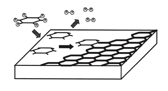
This innovation consists of a set of methodologies for preparing large area (>1 cm2) domains of single-atomic-layer graphite, also called graphene, in single (two-dimensional) crystal form. To fabricate a single graphene layer using chemical vapor deposition (CVD), the process begins with an atomically flat surface of an appropriate substrate and an appropriate precursor molecule containing carbon atoms attached to substituent atoms or groups. These molecules will be brought into contact with the substrate surface by being flowed over, or sprayed onto, the substrate, under CVD conditions of low pressure and elevated temperature. Upon contact with the surface, the precursor molecules will decompose. The substituent groups detach from the carbon atoms and form gas-phase species, leaving the unfunctionalized carbon atoms attached to the substrate surface. These carbon atoms will diffuse upon this surface and encounter and bond to other carbon atoms. If conditions are chosen carefully, the surface carbon atoms will arrange to form the lowest energy single-layer structure available, which is the graphene lattice that is sought.
Another method for creating the graphene lattice includes metal-catalyzed CVD, in which the decomposition of the precursor molecules is initiated by the catalytic action of a catalytic metal upon the substrate surface. Another type of metal-catalyzed CVD has the entire substrate composed of catalytic metal, or other material, either as a bulk crystal or as a think layer of catalyst deposited upon another surface. In this case, the precursor molecules decompose directly upon contact with the substrate, releasing their atoms and forming the graphene sheet.
Atomic layer deposition (ALD) can also be used. In this method, a substrate surface at low temperature is covered with exactly one monolayer of precursor molecules (which may be of more than one type). This is heated up so that the precursor molecules decompose and form one monolayer of the target material.
This work was done by Michael Bronikowski and Harish Manohara of Caltech for NASA's Jet Propulsion Laboratory.
In accordance with Public Law 96-517, the contractor has elected to retain title to this invention. Inquiries concerning rights for its commercial use should be addressed to:
Innovative Technology Assets Management
JPL
Mail Stop 202-233
4800 Oak Grove Drive
Pasadena, CA 91109-8099
E-mail:
Refer to NPO-45298, volume and number of this NASA Tech Briefs issue, and the page number.
This Brief includes a Technical Support Package (TSP).
Fabricating Large-Area Sheets of Single-Layer Graphene by CVD
(reference NPO-45298) is currently available for download from the TSP library.
Don't have an account?
Overview
The document is a technical support package from NASA's Jet Propulsion Laboratory (JPL) detailing the fabrication of large-area sheets of single-layer graphene using Chemical Vapor Deposition (CVD). It outlines the innovative methods and processes involved in producing high-quality graphene, which has significant implications for various technological and scientific applications.
Graphene, a single layer of carbon atoms arranged in a hexagonal lattice, is known for its exceptional electrical, thermal, and mechanical properties. The document emphasizes the importance of starting with an atomically flat substrate and using appropriate precursor molecules that contain carbon atoms. These precursor molecules are introduced to the substrate under controlled conditions of low pressure and elevated temperature. Upon contact, the precursor molecules decompose, releasing substituent groups as gaseous products while leaving carbon atoms bound to the substrate.
The process involves the diffusion of these surface-bound carbon atoms, which then bond to form the desired graphene lattice structure. The document highlights the careful selection of conditions to ensure that the carbon atoms arrange themselves into the lowest energy configuration, resulting in a single-layer graphene sheet.
Illustrative figures, such as Figure 1, depict the growth process of the graphene sheet, showcasing how carbon atoms interact and bond at the growing edge of the lattice. The document also mentions various precursor materials, including methane and its derivatives, which can be utilized in the CVD process.
Overall, this technical support package serves as a comprehensive guide for researchers and technologists interested in the production of graphene, providing insights into the methodologies, potential applications, and the significance of this material in advancing various fields. The information is part of NASA's Commercial Technology Program, aimed at disseminating aerospace-related developments with broader technological implications. The document concludes with contact information for further inquiries related to research and technology in this area, emphasizing the collaborative nature of innovation at JPL.