
A process has been proposed for growing carbon nanotubes aligned substantially parallel with the nominal planar surfaces of substrates and further aligned with patterns on the substrates. Prior to growth, the patterns would be formed by micro-machining the substrates, which could be silicon or silicon-on-insulator (SOI) wafers. By making it possible to tailor the positions and orientations of individual carbon nanotubes grown on pre-patterned substrates, this process would enable advances in nanotube-based electronic and electromechanical devices.

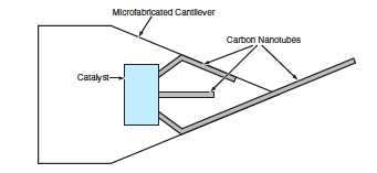
The basic process admits of three main variants, each involving a different technique or combination of techniques to position and orient the growing carbon nanotubes. In the first variant (the basic process), the desired alignment would be enforced by use of in-plane pointed silicon cantilevers protruding from an undercut silicon layer on an SOI substrate (see Figure 1). Part of the upper surface of each cantilever would be coated with a thin film of a suitable catalyst (e.g., Ni, Co, or a suitable metal alloy or compound).
On the basis of prior experiments on the growth of nanotubes, it is expected that (1) the nanotubes will tend to nucleate at random times and locations, such that multiple tubes may grow out of each catalyst film, and (2) because of attractive van der Waals forces, the nanotubes will tend to grow along the cantilever surfaces and edges. It is also anticipated that if the tip of a growing nanotube reaches the tip of the cantilever, further growth would likely cause the nanotube to protrude from the tip because strain-energy cost of bending the nanotube to the small tip radius would exceed the energy of van der Waals attraction (see Figure 2).
In the second variant of the process, the micro-machined patterns would comprise narrow, etched trenches in silicon wafers. Enhanced van der Waals forces at the edges of the trenches would preferentially align the growing nanotubes.
In the third variant of the process, electric fields would be used to align the growing nanotubes. In this case, each substrate would be prepared by microfabrication of (1) pointed cantilevers similar to those of the first variant of the process and (2) on-chip electrodes. A bias potential applied during growth would result in a high local electric field between an electrode on the tip of each cantilever and a nearby electrode. The bias circuitry would be designed to prevent the large surges of current that would destroy the growing nanotubes as the interelectrode gaps became bridged by growth of the nanotubes (e.g., by incorporating a large series resistor in the circuit). It may be necessary to adjust the pressure of the CVD gas and/or electrode spacing to prevent electrical discharges between the biased electrodes.
This work was done by Brian Hunt, Daniel Choi, Michael Hoenk, Robert Kowalczyk, and Flavio Noca of Caltech for NASA’s Jet Propulsion Laboratory.
In accordance with Public Law 96-517, the contractor has elected to retain title to this invention. Inquiries concerning rights for its commercial use should be addressed to
Intellectual Property group
JPL
Mail Stop 202-233
4800 Oak Grove Drive
Pasadena, CA 91109
(818) 354-2240
Refer to NPO-30205, volume and number of this NASA Tech Briefs issue, and the page number.
This Brief includes a Technical Support Package (TSP).
Growing Carbon Nanotubes Aligned with Patterns
(reference NPO-30205) is currently available for download from the TSP library.
Don't have an account?
Overview
The document outlines a technical disclosure regarding the growth of carbon nanotubes (CNTs) aligned with specific patterns, developed under a NASA contract. Carbon nanotubes are recognized for their exceptional properties, including a nanometer-scale diameter, high electrical conductivity, and remarkable mechanical strength, with a Young's modulus of approximately 1 TPa. These characteristics make them ideal candidates for various nanoscale electronic and mechanical applications. However, a significant challenge in utilizing CNTs is achieving controlled placement and orientation during their growth.
The document highlights that chemical vapor deposition (CVD) is the most suitable method for producing CNTs for sensor and electronic applications. CVD involves decomposing a carbon-containing gas, such as methane, at high temperatures (700-900°C) on a substrate coated with a catalyst film. Despite the effectiveness of CVD, previous studies have often resulted in disordered nanotube films, which limits their practical application.
To address this issue, the inventors propose novel methods for controlling the growth of CNTs. They suggest using pre-patterned surface features, such as pointed cantilevers, to direct the lateral growth of nanotubes along the substrate or over trenches. This approach aims to achieve better alignment and orientation of the nanotubes, which is crucial for their integration into functional devices. Additionally, the inventors mention the potential use of a local electric field generated by biased electrodes on the substrate to further enhance the growth process.
The document also references related work in the field, noting that while some researchers have demonstrated in-plane growth of nanotubes between catalyst patterns, the alignment achieved has been largely random. The proposed methods aim to improve upon these previous efforts by providing a more controlled and directed growth process.
Overall, this technical disclosure presents a significant advancement in the field of nanotechnology, particularly in the controlled growth of carbon nanotubes. The techniques described could lead to improved performance in electronic and mechanical devices, making them more viable for practical applications. The work was conducted at the Jet Propulsion Laboratory (JPL) and is part of ongoing research to harness the unique properties of carbon nanotubes for future technological innovations.