
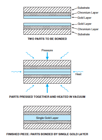
A technique of thermocompressive gold-to-gold diffusion bonding at relatively low temperature has been devised to provide stable, uniform, strong bonds between struc- tural components of microelectromechanical systems. The technique can also be used for vacuum sealing of microscopic cavities. Unlike some other metal-to-metal diffusion bonding techniques, this technique does not entail significant outgassing or the formation of intermetallic compounds. The technique is suitable for bonding of parts made of silicon, quartz, low-thermal-expansion glass, and other materials that can withstand the relatively mild rigors of a low-temperature thermocompressive-bonding process. Two parts to be joined by this technique must have faying surfaces that are either flat or shaped to fit each other. In preparation for bonding, each of the faying surfaces is coated with a layer of chromium, then with a layer of gold (see figure). The coating is done by electron-beam evaporation. The coated substrates are cleaned, then clamped together with their gold layers touching in the desired final configuration in a press in a vacuum chamber.
This work was done by Tony K. Tang and Roman Gutierrez of Caltech for NASA’s Jet Propulsion Laboratory.
This invention is owned by NASA, and a patent application has been filed. Inquiries concerning nonexclusive or exclusive license for its commercial development should be addressed to the Patent Counsel, NASA Management Office–JPL (818) 354-7770. Refer to NPO-20076.
This Brief includes a Technical Support Package (TSP).
Low-Temperature Thermocompressive Au-to-Au Diffusion Bonding
(reference NPO-20076) is currently available for download from the TSP library.
Don't have an account?
Overview
The document outlines a novel low-temperature thermocompressive bonding technique developed for microelectromechanical systems (MEMS) using gold as the bonding agent. This method addresses the challenges associated with conventional high-temperature metal-to-metal bonding techniques, which often cannot accommodate the diverse materials used in MEMS devices.
The bonding process involves applying pressure and heat in a vacuum environment to facilitate the diffusion of metal atoms between two components made of the same metallic composition. Specifically, a layer of chromium followed by a layer of gold is e-beam evaporated onto silicon micro-machined components. These components are then cleaned, aligned, and placed in a chamber evacuated to below 10^-5 torr. The components are heated to a temperature range of 100°C to 350°C while compression is applied via a flat piston for at least one hour, resulting in a strong bond.
Key features of this low-temperature bonding technique include:
- Very Low Temperature: The bonding occurs at significantly lower temperatures compared to traditional methods, making it suitable for materials that cannot withstand high heat.
- Uniform Adhesion: The process ensures good and uniform adhesion between the bonded layers.
- Vacuum Seal Bonding: It provides a hermetic seal, essential for many MEMS applications.
- No Intermetallic Formation: The technique avoids the formation of intermetallic compounds, which can compromise bond integrity.
- No Outgassing: The bonding agent exhibits low outgassing characteristics, crucial for vacuum applications.
- Electrical and Thermal Conductivity: The bond maintains good electrical and thermal conductivity, which is vital for electronic applications.
- High-Temperature Cycling Resistance: The bond can withstand high-temperature cycling, enhancing the durability of the assembled devices.
The motivation behind this development stems from the need for stable, high-strength bonds in MEMS devices that often require the assembly of components made from different materials. Conventional bonding techniques, such as metal-eutectic bonding and soldering, do not meet all the necessary criteria simultaneously. This innovative bonding process allows for the fabrication of unique MEMS devices that require vacuum cavity enclosures and can accommodate various materials without the risk of damage from high temperatures.
Overall, this document presents a significant advancement in bonding technology for MEMS, enabling the creation of more complex and reliable devices for various applications.