
The term “nanophotonics” is used to encompass the scientific study of the interaction of matter and light at the nanometer scale. It is possible to design nanometer scale devices to slow down, enhance, produce, or manipulate light by understanding how light behaves as it travels through, or otherwise interacts with, materials at the nanometer scale. Two applications where nanophotonics have had an impact on society are devices used in optical switching for telecommunications and Organic Light Emitting Diodes (OLEDs) used in display technology and lighting.
As the ability to effectively design and manufacture devices at the nanometer scale increases, the applications for nanophotonics grow. There are many industries that benefit from this science and its continued advancement including computer, telecommunication, biotechnology, and sensing.
One way to picture the interaction of light and matter in a nanophotonic material is to consider a photonic crystal. A photonic crystal is a material that has a nanostructure which affects the motion of electromagnetic energy. Photonic crystals can be used in different applications including telecommunications, security dyes and paints. One very colorful example is color changing paints. A small amount of photonic crystals is added to a base paint resulting in a coating that, depending on the type of light shining on it as well as the viewing angle, appears to change colors. As light travels through the crystal it interacts with the matrix of the material. The way that light interacts with the material can be manipulated by changing the surroundings in which the crystal resides. For example, an electric field can be applied to the material to change the speed at which light travels through it. Manipulation of photonic materials can result in changes in frequency/wavelength as well as intensity.
Another more visual, naturally occurring pseudo-example of the interaction of light and matter can be seen in the iridescent opal. The various colors and changes are due to the Bragg diffraction of light on crystal lattice planes. Bragg diffraction involves the penetration of a material by some form of light. If the material is crystalline and has different layers separated by some uniform distance it is possible to measure the distance between the layers using Bragg’s Law. In Bragg’s Law some of the light is reflected by each of the different layers while some light penetrates within the material. By measuring the differences in the reflected light that comes out from different levels it is possible to determine the distance between these levels using geometry and algebra.
While the applications of nanophotonics are broad, the central theme of the production or manipulation of light through a material constructed at nanoscale dimensions is constant. The purpose of the science of nanophotonic devices is to synergistically combine the intimate interaction of matter and light at the nanometer scale. Leading areas of research include optical and electronic devices. A few examples of devices are on-chip and chip-to-chip interconnects, optical switches, optical waveguides as well as the nonlinear electro-optic devices, modulators, and waveguides. Ultimately optical devices are trying to take advantage of the wave type property of light. It is possible to use both constructive and destructive interference to modulate a light signal.
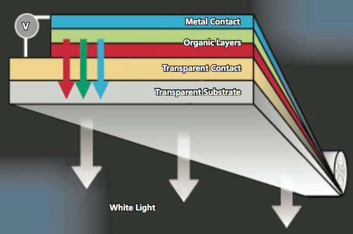
Some nanophotonic applications involve interacting with light while others involve the emission of light. Examples of nanophotonic applications that involve the emission of light include quantum dots, OLED, sensor applications, and next generation silicon based emitting devices. Quantum dots are luminescent materials that are currently being studied for light emitting processes. Quantum dots are typically made from inorganic materials including cadmium, indium, lead, phosphorus, selenium, and sulfur. The wavelength of light produced from these materials is dependent on the size of the particle that is emitting the light. It is possible to produce light of specific color by strictly controlling the size of the quantum dot. General quantum dot particle sizes range from 10 to 100 nanometers in diameter.
An area in the science of nanophotonics that has been attracting attention and increasing promise over the last fifteen years is the area of two-photon materials and processes. Two-photon nanophotonics is the process involving the simultaneous absorption of two low energy photons by a material to produce a higher energy state (excited state). In theory, the energy of the excited state in the target molecule is equal to the sum of the two photons. Applications for two-photon materials include fluorescent imaging, sensitization, and next generation nanolithography.
This absorption process is very weak and is classified as a 3rd order nonlinear optical process. The intensity of simultaneously absorbing two photons to form a high energy state is extremely weak and requires a laser of a certain threshold in intensity. There are many applications that take advantage of the requirements for two-photon processes to take place. When two low power laser sources, where neither of which have sufficient power to initiate a two-photon process, are trained on an object at a 45° angle, there is sufficient photon flux to initiate a two-photon process at the point where the two laser sources cross. The result is a targeted activation within an object. An application of this targeted two-photon process is the creation of 2D or 3D objects through the use of two-photon initiated polymerization reactions. Photo Dynamic Therapy (PDT) is a well established example of the application of two-photon processes. PDT involves using light to activate photoactive medicines that are introduced into the body. PDT is used to treat different medical conditions including certain types of cancer. Recent and continued improvements in the materials, resolution, and fabrication efficiency will soon make many materials manufactured from two-photon processes a widespread reality.
Nanotechnology is a fast growing field that will continue to have an impact on the daily life of us all. Improvements in efficiency and manufacturing technologies will allow nanophotonic based applications to be found in every home in the future. Lighting panels based on OLEDs, light activated medicines delivered directly to the needed location in the body, and flexible display screens that can be rolled or folded are just some of the near-term products coming. Nanophotonics allows for the possibility of processes running at the speed of light instead of being limited to the speed of electrons.
This article was written by Gregory D. Phelan, Affiliate Associate Professor, Center for Materials and Devices for Information Technology Research, University of Washington (Seattle, WA). For more information, contact Mr. Phelan at