Find the latest developments in Photonics & Imaging essential to both Commercial & Government applications. Get expert solutions for imaging systems, machine vision, visualization software, human machines (HMIs), plus advances in infrared cameras and display monitoring.
Harvard research breakthrough could speed development of room‐temperature quantum computers…New generation of ultra‐lightweight, high‐res space cameras takes flight…NASA LiDAR advance gives...
Ongoing use of the laser has broadened the horizon of aerospace and defense capabilities by enabling the warfighter and through additive manufacturing processes that result in...
This article highlights requirements for an IR imaging C-UAS platform and examines the design of one state-of-the-art lens system for this application. Read on to learn more.
As electric vehicle designs change and production targets grow even more aggressive, advanced laser welding technologies have continued to evolve to help manufacturers be more efficient and stay competitive. Read on to learn more about it.
We here at Tech Briefs want to remedy that toxic part of the holidays. So, we put together a list of terrific gift ideas for anyone — but especially the engineer — in your life.
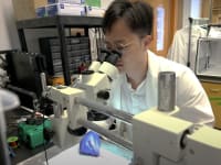
Miniaturization ranks as the driving force behind the semiconductor industry. The tremendous gains in computer performance since the 1950s are largely due to the fact that ever smaller...
See the products of tomorrow, including a drone with flapping wings that can locate and hover around a moving light like a moth to a flame; a new multi-layered metalens design that could revolutionize portable optics in devices like phones, drones, and satellites; and more.
Researchers have successfully demonstrated the U.K.’s first long-distance ultra-secure transfer of data over a quantum communications network, including the U.K.’s first long-distance quantum-secured video call. Read on to learn more.
NASA Goddard Space Flight Center has developed a Space Qualified Rover LiDAR (SQRLi) system that will improve rover sensing capabilities in a small, lightweight package. The new SQRLi package is developed to survive the hazardous space environment and provide valuable image data during planetary and lunar rover exploration. Read on to learn more about it.
NASA's Glenn Research Center has developed a method of using entangled-photon pairs to produce highly secure mobile communications that require mere milliwatts of power. Read on to learn more.
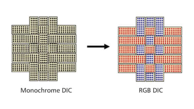
Innovators at NASA Johnson Space Center have developed a technology that can isolate a single direction of tensile strain in biaxially woven material. This is accomplished using traditional digital image correlation (DIC) techniques in combination with custom red-green-blue (RGB) color filtering software. Read on to learn more.
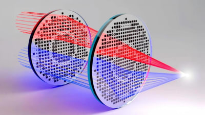
Optics researchers in the Harvard John A. Paulson School of Engineering and Applied Sciences created specially designed metasurfaces — flat devices etched with nanoscale light-manipulating patterns — to act as ultra-thin upgrades for quantum-optical chips and setups. Read on to learn more.
Researchers at the University of California San Diego have developed a soft robotic skin that enables vine robots that are just a few millimeters wide to navigate convoluted paths and fragile environments. Read on to learn more.
Photonic processor enables ultrafast AI computations…how new polishing technique could revolutionize optical manufacturing…facial mapping technology is a leap forward in augmented reality. Read...
Researchers have been developing computers that deploy light, or photons, rather than electricity to power storage and calculations. These light-based computers...
NLM Photonics has confirmed that its patented silicon organic hybrid (SOH) photonic chips, featuring Selerion-HTX™ and JRD1, have successfully arrived at the International...
A wearable device, a-Heal, designed at the University of California, Santa Cruz, aims to expedite the entire healing process. It uses a tiny camera and AI to detect the stage of healing and deliver treatment in the form of medication or an electric field.
Researchers have developed a soft robotic skin that enables vine robots a few millimeters wide to navigate convoluted paths and fragile environments. To accomplish...
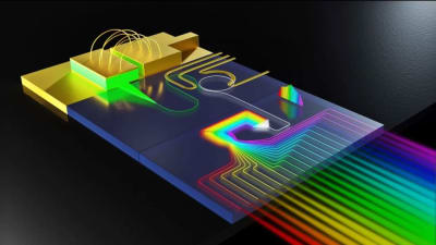
A few years ago, researchers in Michal Lipson’s Columbia Engineering lab noticed something remarkable. They were working on a project to design high-power chips that could...
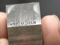
See what's new on the market, including Boker’s stamped metal components custom manufactured to fit into developed mold designs; the CRH03 tactical-grade gyroscope from Silicon Sensing Systems; Keysight Technologies' enhanced physical layer compliance test solution for high-definition multimedia interface; and more.
Lasers vs. drones: military demonstrates new tech…high-‐flying uncrewed solar aircraft aces key test…the next frontier for autonomous UAVs. Read about these and other developments in this...
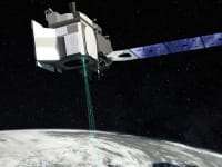
Critical advantages and challenges of using laser communications in space…the future of EMI protection for military aircraft…new "micro comb" chips promise to improve GPS accuracy. Read about these...
Researchers have used the centuries-old idea of pinhole imaging to create a high-performance mid-infrared imaging system without lenses. The new camera can capture extremely clear pictures over a large range of distances and in low light, making it useful for situations that are challenging for traditional cameras.
As NASA embarks on the next era of human space exploration — returning to the Moon and venturing beyond — reliable, fast, and secure space-based communication systems will...


 Blog: Lighting
 INSIDER: Energy
 Blog: Power
 Quiz: Energy
 Blog: Lighting Technology
 Blog: Data Acquisition
 On-Demand Webinars: Electronics & Computers
 Upcoming Webinars: Automotive
 Upcoming Webinars: Test & Measurement
 Upcoming Webinars: Defense
 Upcoming Webinars: Sensors/Data Acquisition