
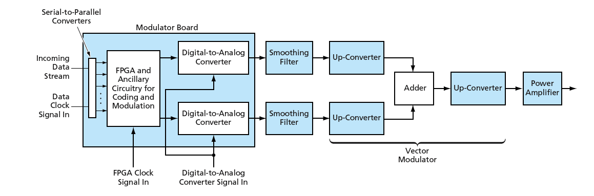
A modulator circuit board has recently been developed to be used in conjunction with a vector modulator to generate any of a large number of modulations for bandwidth-efficient radio transmission of digital data signals at rates than can exceed 100 Mb/s. The modulations include quadrature phase-shift keying (QPSK), offset quadrature phase-shift keying (OQPSK), Gaussian minimum-shift keying (GMSK), and octonary phase-shift keying (8PSK) with square-root raised-cosine pulse shaping. The figure is a greatly simplified block diagram showing the relationship between the modulator board and the rest of the transmitter. The role of the modulator board is to encode the incoming data stream and to shape the resulting pulses, which are fed as inputs to the vector modulator. The combination of encoding and pulse shaping in a given application is chosen to maximize the bandwidth efficiency.
At the time of reporting the information for this article, a prototype of the modulator board had been tested in laboratories, and tests in a two-way ground-to-spacecraft communication link were planned. Although the modulator board was conceived for original use in spacecraft-to-spacecraft and spacecraft-to-ground communications, there are potential terrestrial uses in microwave tower-to-tower links and aircraft remote sensing systems.
By making it possible to implement many different high-rate modulators in the same piece of hardware, the underlying design concepts of this modulator can be expected to afford economies of scale: It would cost less to manufacture many identical modulator hardware units to satisfy market demands for many types of modulators than to manufacture smaller numbers of specialized modulator units having different designs.
This work was done by Andrew Gray, Dennis Lee, Norman Lay, and Craig Cheetham of Caltech; Wai Fong, Pen-Shu Yeh, Robin King, and Parminder Ghuman of Goddard Space Flight Center; and Scott Hoy and Dave Fisher of Lockheed-Martin for NASA’s Jet Propulsion Laboratory.
In accordance with Public Law 96-517, the contractor has elected to retain title to this invention. Inquiries concerning rights for its commercial use should be addressed to:
Innovative Technology Assets Management
JPL
Mail Stop 202-233
4800 Oak Grove Drive
Pasadena, CA 91109-8099
(818) 354-2240
E-mail:
Refer to NPO-40807, volume and number of this NASA Tech Briefs issue, and the page number.
This Brief includes a Technical Support Package (TSP).
Multi-Modulator for Bandwidth-Efficient Communication
(reference NPO-40807) is currently available for download from the TSP library.
Don't have an account?
Overview
The document outlines a Technical Support Package for the Multi-Modulator for Bandwidth-Efficient Communication, developed under NASA's Commercial Technology Program. It details the advancements in modulation techniques aimed at enhancing communication efficiency for aerospace applications. The focus is on creating a Multi-modulator Flight ASIC that can support high data throughput rates, exceeding 600 Mbps, which is crucial for current and future space missions.
Key elements of the project include an overview of bandwidth-efficient modulation techniques such as GMSK (Gaussian Minimum Shift Keying), 8-PSK (8 Phase Shift Keying) with Trellis Coded Modulation (TCM), and Filtered OQPSK (Offset Quadrature Phase Shift Keying). The document discusses the design and implementation processes, including the use of Field Programmable Gate Arrays (FPGAs) for prototyping and the eventual transition to Application-Specific Integrated Circuits (ASICs).
The requirements for the system are clearly defined, with a digital sampling and processing rate range of 100 Kbps to 300 Mbps for 8-PSK without coding, and a maximum data rate of 200 Mbps for GMSK and O-QPSK. The document specifies the necessary digital-to-analog (D/A) converter rates, which must reach up to 400 MHz for optimal performance, and outlines the architecture for modulation generation, including the use of smoothing filters and power amplifiers.
Additionally, the document emphasizes the importance of a parallel Hardware Description Language (HDL) realization of the modulation suite, which aids in the efficient design and testing of the system. It also highlights the complexity estimates and gate counts associated with the modulation techniques, providing insights into the VLSI (Very Large Scale Integration) design process.
The Technical Support Package serves as a comprehensive resource for understanding the technological advancements in bandwidth-efficient communication, showcasing NASA's commitment to innovation in aerospace technology. It invites further inquiries and collaboration through the contact information provided, emphasizing the potential for broader applications of the research and technology developed in this project. Overall, the document encapsulates a significant step towards improving communication capabilities in space exploration.