
An all-digital demodulator has been developed for receiving radio signals with multigigahertz carrier frequencies phase-modulated with digital data signals at bit rates of hundreds of millions of bits per second. The phase modulation could be either binary phase-shift keying (BPSK) or quadrature phase-shift keying (QPSK), including QPSK employing bandwidth efficient pulse-shaping methods. The demodulator has been implemented in complementary metal oxide semiconductor (CMOS) application-specific integrated circuit (ASIC) configured to utilize algorithms that process signal data in multiple parallel streams.
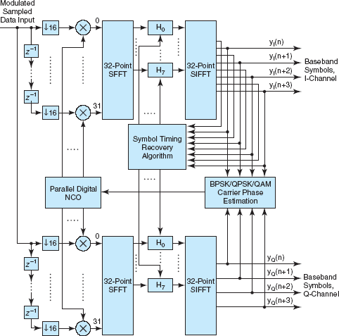
The present all-digital demodulator is characterized by an advanced parallel receiver (APRX) architecture (see figure), which replaces the receiver functions of the parallel receiver (PRX) architecture reported in “Parallel Digital Demodulators Using Multirate Filter Banks” (NPO-19620), NASA Tech Briefs, Vol. 20, No. 10 (October 1996), page 65. The APRX architecture is essentially one of time-varying frequency-domain detection filtering and symbol-timing correction.
Upstream of this demodulator, the received analog signal is converted to an intermediate frequency (IF) suitable for analog-to-digital (A/D) conversion, band-pass filtered, then digitized at a rate of 4 samples per symbol. The band-pass filtering rejects some noise and prevents the aliasing that would otherwise occur after A/D conversion. The digital signal is split into 32 parallel paths, decimated by 16 on each path, and digitally mixed on each path with a replica of the sampled IF carrier signal. The discrete Fourier transform (DFT) of the resulting 32 data points is then taken, via a specialized fast Fourier transform (SFFT), and multiplied by the one element of a bank of frequency-domain-matched filters. The correct matched filter is chosen by the closed-loop symbol timing recovery algorithm (see figure).
To suppress the double-frequency terms generated in mixing to baseband, low-pass filtering is performed, zeroing out the middle 16 components (which correspond to the high-frequency terms) in the frequency domain. Then the inverse discrete Fourier transform (IDFT) is computed, via the specialized inverse fast Fourier transform (SIFFT), and the middle 16 parallel outputs (which are unaliased and correspond to 4 symbol periods) are used for detection, tracking, and other purposes.
The foregoing process is repeated once every 16 cycles of the A/D-converter clock. The 16 points in the SIFFT output are 16 samples of a convolution of the input sequence with the matchedfilter impulse-response function. Among these 16 samples are 4 baseband symbols that correspond to the peak signal-tonoise- ratio outputs of the matched filter.
Theoretical analysis, computational simulations, laboratory tests, and live satellite downlinks have shown that the error-rate performance of the APRX demodulator can be expected to be equivalent, and in some cases superior, to that of a conventional serial-processing digital receiver. In comparison with the PRX architecture, the APRX architecture can be implemented with significantly reduced complexity. In comparison with traditional serial digital receivers, the APRX demodulator ASIC can process much higher data rates. The next generation implementation of the APRX ASIC is currently being developed to process higher order modulations and data rates in excess of 2 billion bits per second.
This work was done by Parminder Ghuman, Scott Hoy, and Gerald Grebowsky of Goddard Space Flight Center and Andrew Gray and Meera Srinivasan of Caltech for NASA’s Jet Propulsion Laboratory. For further information, access the Technical Support Package (TSP) free on-line at www.nasatech.com/tsp under the Electronic Components and Systems category. NPO-21230
This Brief includes a Technical Support Package (TSP).
Parallel-Processing High-Rate Digital Demodulator ASIC
(reference NPO-21230) is currently available for download from the TSP library.
Don't have an account?
Overview
The document presents the architecture and development of a High Rate Digital Demodulator (HRDD) ASIC designed for demodulating BPSK (Binary Phase Shift Keying) and QPSK (Quadrature Phase Shift Keying) modulated data at data rates of up to 600 Megabits per second. This technology is particularly relevant for NASA missions, where the demand for high data rates is rapidly increasing.
The HRDD ASIC employs an all-digital processing approach, which offers several advantages over traditional analog or mixed-signal solutions. These advantages include increased flexibility, reliability, and reduced reproduction costs. The document highlights the challenges associated with conventional serial digital processing, which requires high processing rates that are often impractical with current technologies. Instead, the HRDD utilizes parallel processing algorithms that allow the demodulator to operate at a clock rate significantly lower than the data rate, making it feasible to implement using CMOS technology.
The design process for the HRDD involved several stages: algorithmic development, software simulations, hardware prototyping in reprogrammable hardware, and the final development of a single 800K gate CMOS ASIC. The architecture requires two identical ASICs for in-phase (I) and quadrature (Q) channel processing. The input signals are processed through a series of steps, including demultiplexing, digital mixing, and frequency domain conversion via a modified 32-point Discrete Fourier Transform (DFT). The outputs are then filtered to eliminate unwanted frequency components and perform symbol detection.
The document emphasizes the importance of using parallel processing to handle the high sampling rates required for effective demodulation. For instance, to demodulate data at 300 Megabits per second, a sampling rate of 1,200 million samples per second is necessary, which is achievable with the HRDD's architecture running at a clock rate of only 75 MHz.
Overall, the HRDD represents a significant advancement in digital demodulation technology, enabling high-performance processing for future NASA missions while maintaining cost-effectiveness and flexibility. The work was conducted under the auspices of NASA and the Jet Propulsion Laboratory, showcasing a commitment to innovation in space communication technologies.