
A complementary metal oxide/semiconductor (CMOS) image detector now undergoing development is designed to exhibit less cross-talk and greater full-well capacity than do prior CMOS image detectors of the same type. Imagers of the type in question are designed to operate from low-voltage power supplies and are fabricated by processes that yield device features having dimensions in the deep submicron range.
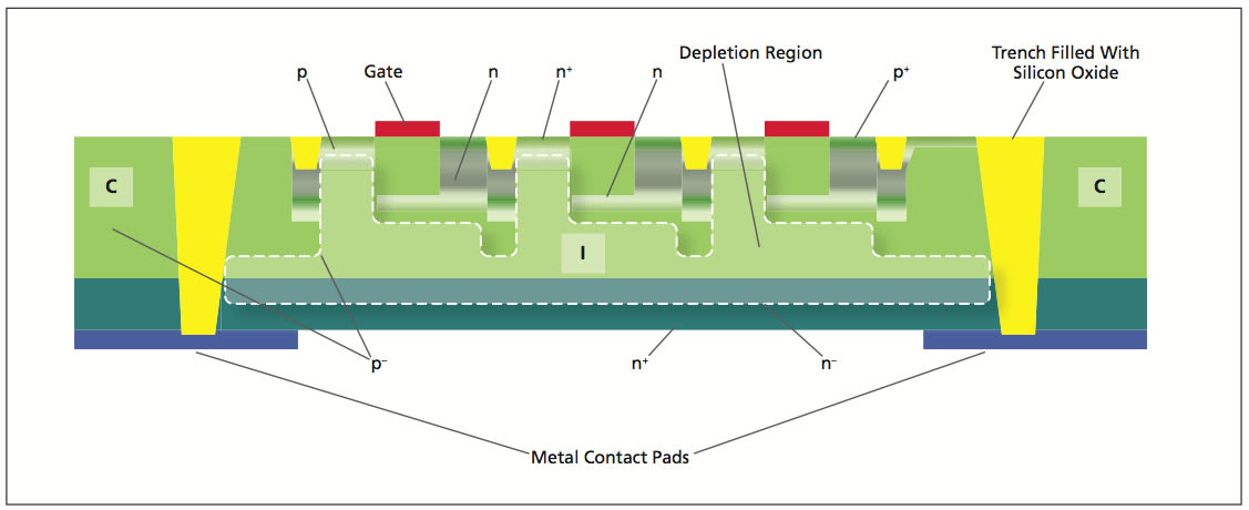
The figure shows a partial cross section of the structure in the device layer of the present developmental CMOS imager. (In a practical imager, the device layer would sit atop either a heavily doped silicon substrate or a thin silicon oxide layer on a silicon substrate, not shown here.) The imager chip is divided into two areas: area C, which contains readout circuits and other electronic circuits; and area I, which contains the imaging (photodetector and photogenerated-charge-collecting) pixel structures. Areas C and I are electrically isolated from each other by means of a trench filled with silicon oxide.
The electrical isolation between areas C and I makes it possible to apply different supply potentials to these areas, thereby enabling optimization of the supply potential and associated design features for each area. More specifically, metal oxide semiconductor field-effect transistors (MOSFETs) that are typically included in CMOS imagers now reside in area C and can remain unchanged from established designs and operated at supply potentials prescribed for those designs, while the dopings and the lower supply potentials in area I can be tailored to optimize imager performance.
In area I, the device layer includes an n+-doped silicon layer on which is grown an n–-doped silicon layer. A p–-doped silicon layer is grown on top of the n–-doped layer. The total imaging device thickness is the sum of the thickness of the n+, n, and p– layers. A pixel photodiode is formed between a surface n+ implant, a p implant underneath it, the aforementioned p– layer, and the n and n+ layers. Adjacent to the diode is a gate for transferring photogenerated charges out of the photodiode and into a floating diffusion formed by an implanted p+ layer on an implanted n-doped region. Metal contact pads are added to the back-side for providing back-side bias.
The n– and p– doping concentrations are chosen such that everywhere in area I, a depletion region exists between the n– and p– layers. This depletion region enables electrical isolation between the several front (top) doped regions and the back (bottom) n and n+ layers. Consequently, the bias potentials applied to the top of the diode and the adjacent transfer gate can be different from the bias applied to the bottom. Thus, while CMOS-compatible potentials (e.g., 3 V) are applied at the top, the bottom of the structure can be biased to greater potential (e.g., 5 V) via the back-side metal contact pads to completely deplete the photodiode. The resulting depletion region is indicated in the figure as the area enclosed by the dashed outline. Complete depletion of the photodiode results in collection of charge carriers (holes in this case) under the influence of an electric field, and hence, a significant reduction of cross-talk. Complete depletion also increases the charge-storage volume, and, hence, the charge-handling capacity. Thus, the structure described here provides for large depletion width around each photodiode, independent of the CMOS power-supply voltage and pixel size.
This work was done by Bedabrata Pain and Thomas J. Cunningham of Caltech for NASA’s Jet Propulsion Laboratory. For more information, download the Technical Support Package (free white paper) at www.techbriefs.com/tsp under the Electronics/Computers category. In accordance with Public Law 96-517, the contractor has elected to retain title to this invention. Inquiries concerning rights for its commercial use should be addressed to:
Innovative Technology Assets Management
JPL Mail Stop 202-233 4800 Oak Grove Drive Pasadena, CA 91109-8099 E-mail:
Refer to NPO-45964, volume and number of this NASA Tech Briefs issue, and the page number.
This Brief includes a Technical Support Package (TSP).

CMOS Imager Has Better Cross-Talk and Full-Well Performance
(reference NPO-45964) is currently available for download from the TSP library.
Don't have an account?
Overview
The document discusses advancements in CMOS (Complementary Metal-Oxide-Semiconductor) imager technology, specifically focusing on improvements in cross-talk and charge handling capacity. It highlights a new structure and method designed to increase the depletion width and enhance the performance of back-illuminated CMOS imagers, which are particularly challenged by the need for photo-generated carriers to traverse the entire thickness of the device.
The key innovation involves the design of the pixel diode, which is formed between various silicon layers: an n+ surface implant, a p-type implant beneath it, a p- epitaxial layer, and an n-/n+ layer. This configuration allows for a continuous depletion region between the n- and p- layers, enabling high voltage back-biasing. This results in complete depletion of the photodiode, which significantly reduces electrical cross-talk and increases the charge storage volume, thereby enhancing the charge handling capacity.
The document explains that the structure is divided into two electrically isolated sections: the imaging area and the circuits area, separated by trench oxide isolation. This design allows different voltages to be applied to the imaging area compared to the circuits area, optimizing performance without altering the operation of the MOSFETs in the circuits area.
The report emphasizes that traditional CMOS imagers, particularly those with pinned photodiodes, suffer from reduced charge handling capacity and increased cross-talk due to lower power supply voltages. This limitation restricts the maximum internal electric field and, consequently, the depletion width. The new structure addresses these issues by allowing for a larger depletion width, independent of the CMOS power supply voltage and pixel scaling.
Figures included in the document illustrate the potential profiles and structural layout of the CMOS imager, demonstrating the presence of an electric field for efficient carrier collection and the potential bucket for storing holes in the photodiode area. The findings suggest that the new design can significantly improve the performance of CMOS imagers, making them more effective for various applications, particularly in back-illuminated configurations.
Overall, the document presents a promising advancement in imaging technology that could lead to better performance in future CMOS imagers, enhancing their utility in scientific and commercial applications.