
A generic design and a corresponding operating sequence have been developed for increasing the linear-response dynamic range of a complementary metal oxide/semiconductor (CMOS) image sensor. The design provides for linear calibrated dual-gain pixels that operate at high gain at a low signal level and at low gain at a signal level above a preset threshold. Unlike most prior designs for increasing dynamic range of an image sensor, this design does not entail any increase in noise (including fixed-pattern noise), decrease in responsivity or linearity, or degradation of photometric calibration.
The figure is a simplified schematic diagram showing the circuit of one pixel and pertinent parts of its column readout circuitry. The conventional part of the pixel circuit includes a photodiode having a small capacitance, CD. The unconventional part includes an additional larger capacitance, CL, that can be connected to the photodiode via a transfer gate controlled in part by a latch.
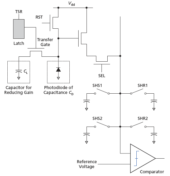
In the high-gain mode, the signal labeled TSR in the figure is held low through the latch, which also helps to adapt the gain on a pixel-by-pixel basis. Light must be coupled to the pixel through a microlens or by back illumination in order to obtain a high effective fill factor; this is necessary to ensure high quantum efficiency, a loss of which would minimize the efficacy of the dynamic-range-enhancement scheme. Once the level of illumination of the pixel exceeds the threshold, TSR is turned on, causing the transfer gate to conduct, thereby adding CL to the pixel capacitance. The added capacitance reduces the conversion gain, and increases the pixel electron-handling capacity, thereby providing an extension of the dynamic range.
By use of an array of comparators also at the bottom of the column, photocharge voltages on sampling capacitors in each column are compared with a reference voltage to determine whether it is necessary to switch from the high-gain to the low-gain mode. Depending upon the built-in offset in each pixel and in each comparator, the point at which the gain change occurs will be different, adding gain dependent fixed pattern noise in each pixel. The offset, and hence the fixed pattern noise, is eliminated by sampling the pixel readout charge four times by use of four capacitors (instead of two such capacitors as in conventional design) connected to the bottom of the column via electronic switches SHS1, SHR1, SHS2, and SHR2, respectively, corresponding to high and low values of the signals TSR and RST. The samples are combined in an appropriate fashion to cancel offset-induced errors, and provide spurious-free imaging with extended dynamic range.
This work was done by Bedabrata Pain of Caltech for NASA's Jet Propulsion Laboratory. For more information, download the Technical Support Package (free white paper) at www.techbriefs.com/tsp under the Electronics/Computers category.
In accordance with Public Law 96-517, the contractor has elected to retain title to this invention. Inquiries concerning rights for its commercial use should be addressed to:
Innovative Technology Assets Management
JPL
Mail Stop 202-233
4800 Oak Grove Drive
Pasadena, CA 91109-8099
(818) 354-2240
E-mail: This email address is being protected from spambots. You need JavaScript enabled to view it.
Refer to NPO-41897, volume and number of this NASA Tech Briefs issue, and the page number.
This Brief includes a Technical Support Package (TSP).
Increasing Linear Dynamic Range of a CMOS Image Sensor
(reference NPO-41897) is currently available for download from the TSP library.
Don't have an account?
Overview
The document is a Technical Support Package from NASA's Jet Propulsion Laboratory (JPL) detailing an innovation in the field of imaging technology, specifically focusing on the enhancement of the linear dynamic range in CMOS (Complementary Metal-Oxide-Semiconductor) image sensors. Identified by the NTR Number 41897 and referenced as NPO-41897 in NASA Tech Briefs, this innovation aims to improve the performance of CMOS image sensors, which are widely used in various applications, including aerospace, consumer electronics, and scientific imaging.
The linear dynamic range of an image sensor refers to its ability to capture a wide range of light intensities, from very dim to very bright, without losing detail in either extreme. Enhancing this range is crucial for applications where lighting conditions can vary significantly, such as in space exploration or high-contrast environments. The document suggests that advancements in this area could lead to better image quality and more reliable data capture in challenging conditions.
The Technical Support Package is part of NASA's Commercial Technology Program, which aims to disseminate aerospace-related developments that have potential technological, scientific, or commercial applications beyond their original context. This initiative underscores NASA's commitment to fostering innovation and collaboration with the private sector and other organizations.
For further inquiries or detailed information regarding the research and technology discussed in this document, the package provides contact details for the Innovative Technology Assets Management team at JPL. They can be reached via mail or email, indicating a willingness to engage with interested parties for potential partnerships or further exploration of the technology.
The document also includes a notice regarding the proprietary nature of the information contained within, emphasizing compliance with U.S. export regulations and the importance of respecting privately owned rights. It clarifies that the use of any trade names or manufacturers' names is solely for identification purposes and does not imply official endorsement by NASA.
In summary, this Technical Support Package presents a significant advancement in CMOS image sensor technology, highlighting its potential applications and inviting collaboration for further development and commercialization.