
A proposed hybrid ultraviolet (UV) image sensor would comprise a planar membrane array of face-up AlGaN/GaN photodiodes integrated with a complementary metal oxide/semiconductor (CMOS) readout-circuit chip. Each pixel in the hybrid image sensor would contain a UV photodiode on the AlGaN/GaN membrane, metal oxide/semiconductor field-effect transistor (MOSFET) readout circuitry on the CMOS chip underneath the photodiode, and a metal via connection between the photodiode and the readout circuitry (see figure). The proposed sensor design would offer all the advantages of comparable prior CMOS active-pixel sensors and AlGaN UV detectors while overcoming some of the detector limitations of prior (AlGaN/sapphire)/CMOS hybrid image sensors that have been designed and fabricated according to the methodology of flip-chip integration.
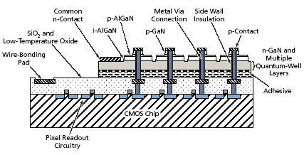
AlGaN is a nearly ideal UV-detector material because its bandgap is wide and adjustable and it offers the potential to attain extremely low dark current. Integration of AlGaN with CMOS is necessary because at present there are no practical means of realizing readout circuitry in the AlGaN/GaN material system, whereas the means of realizing readout circuitry in CMOS are well established. In one variant of the flip-chip approach to integration, an AlGaN chip on a sapphire substrate is inverted (flipped) and then bump-bonded to a CMOS readout circuit chip; this variant results in poor quantum efficiency. In another variant of the flip-chip approach, an AlGaN chip on a crystalline AlN substrate would be bonded to a CMOS readout circuit chip; this variant is expected to result in narrow spectral response, which would be undesirable in many applications. Two other major disadvantages of flip-chip integration are large pixel size (a consequence of the need to devote sufficient area to each bump bond) and severe restriction on the photodetector structure.
The membrane array of AlGaN/GaN photodiodes and the CMOS readout circuit for the proposed image sensor would be fabricated separately. The AlGaN/GaN membrane would be separated from its fabrication substrate by use of laser lift-off or perhaps some other technique that works as well. A temporary holder would be used for lifting off the AlGaN/GaN membrane, transferring this membrane to the CMOS circuit chip, and keeping the front surface of the membrane facing up in the process. The AlGaN/GaN membrane would be bonded to the CMOS chip by use of an adhesive, which could be a polyimide or other, similar material. After curing of the adhesive, the portion of the membrane outside the area of the photodiode arrays would be removed by dry etching. Then the metal via connections between the photodiodes and the CMOS readout circuit would be made in all the pixels.
The performance of the proposed image sensor in solar-blind or visible-blind UV imaging would exceed that achievable in flip-chip integration in two ways:
The face-up orientation of the photodiodes would make it possible for UV photons to be detected at the top layer of the photodetector, where the quality of the photodetector material usually exceeds that of the inner layers. As a result, it should be possible to achieve high quantum efficiency, wide and tailorable spectral response, and low dark current.
The metal via connections in the proposed configuration could be made much narrower than the tens-of-microns-wide bonding bumps of a typical flip-chip configuration. The elimination of the need to devote so much pixel area to bump bonds would enable the design and fabrication of much smaller pixels. Hence, it would be possible to achieve greater spatial resolution of the image and to fit more pixels into a given image area.
This work was done by Xinyu Zheng and Bedabrata Pain of Caltech for NASA’s Jet Propulsion Laboratory. For further information, access the Technical Support Package (TSP) free on-line at www.techbriefs.com/tsp under the Electronics/Computers category.
In accordance with Public Law 96-517, the contractor has elected to retain title to this invention. Inquiries concerning rights for its commercial use should be addressed to:
Innovative Technology Assets Management
JPL
Mail Stop 202-233
4800 Oak Grove Drive
Pasadena, CA 91109-8099
(818) 354-2240
E-mail: This email address is being protected from spambots. You need JavaScript enabled to view it.
Refer to NPO-35079, volume and number of this NASA Tech Briefs issue, and the page number.
This Brief includes a Technical Support Package (TSP).
Hybrid UV Imager Containing Face-Up AlGaN/GaN Photodiodes
(reference NPO-35079) is currently available for download from the TSP library.
Don't have an account?
Overview
The document is a Technical Support Package from NASA, specifically detailing the Hybrid UV Imager that incorporates Face-Up AlGaN/GaN Photodiodes. This technology is part of NASA's efforts to advance aerospace-related developments with broader technological and commercial applications.
The imager features a unique design that integrates a UV photodetective membrane with a complementary metal-oxide-semiconductor (CMOS) read-out circuit. This configuration allows for high-performance UV detection while overcoming limitations associated with traditional CMOS active pixel sensors (APS) and AlGaN UV detectors. The face-up design enhances the device's capabilities in high rejection UV detection and efficient signal read-out.
The document outlines the processing flow for fabricating the AlGaN/GaN photodiode array, which includes the creation of n- and p-contacts and the use of laser lift-off techniques to transfer the photodiode membrane from a sapphire substrate. This method allows for the production of a high-quality photodiode array that can operate effectively in the UV spectrum.
One of the key advantages of this hybrid imager is its wide and tunable coverage over the UV spectrum, with the ability to detect wavelengths ranging from 400 nm to below 100 nm. This flexibility is crucial for various applications, including environmental monitoring, space exploration, and other scientific endeavors where UV detection is essential.
The document also highlights the integration of advanced signal processing capabilities, such as addressable sampling, zooming, analog-to-digital conversion, and wireless communication, all within a single chip. This integration not only improves the functionality of the imager but also enhances its resolution and quantum efficiency, making it superior to traditional flip-chip integration methods.
Overall, the Hybrid UV Imager represents a significant advancement in UV imaging technology, combining innovative design with practical applications. The document serves as a resource for understanding the technical aspects and potential uses of this cutting-edge technology, emphasizing NASA's commitment to fostering innovation in aerospace and beyond. For further information, the document provides contact details for the NASA Scientific and Technical Information Program Office, encouraging exploration of additional resources related to this field.