
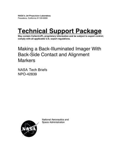
A design modification and a fabrication process that implements the modification have been conceived to solve two problems encountered in the development of back-illuminated, back-side-thinned complementary metal oxide/semiconductor (CMOS) image-detector integrated circuits. With respect to such an integrated circuit to be fabricated on a silicon substrate, the two problems are (1) how to form metal electrical-contact pads on the back side that are electrically connected through the thickness in proper alignment with electrical contact points on the front side and (2) how to provide alignment keys on the back side to ensure proper registration of backside optical components (e.g., microlenses and/or color filters) with the frontside pixel pattern. (In this special context, "front side" signifies that face of the substrate upon which the pixel pattern and the associated semiconductor devices and metal conductor lines are formed.)
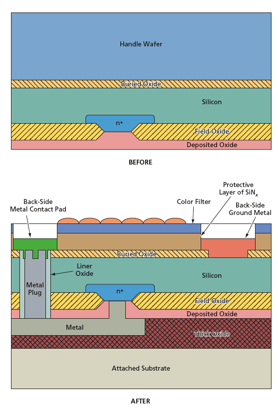
The fabrication process for implementing this design modification would be complex and would be subject to variation as needed for different image-detector applications. Immediately before the beginning of this process, the integrated circuitry would already have been fabricated on the front side of the substrate, as shown in the upper part of the figure. In terms that are necessarily oversimplified for the sake of brevity, the process can be summarized as follows: Through multiple steps of patterning, etching, and deposition, holes through the substrate would be formed at the desired frontside locations and the metal plugs and their protrusions would be formed in the holes. In subsequent steps, the back-side metal pads would be deposited on the metal plug protrusions, then color filters and/or microlenses would be formed between and in alignment with the metal contact pads, yielding the device structure shown in the lower part of the figure. (Not shown in the figure is a back-side antireflection coat that would be added near the end of the process.)
This work was done by Bedabrata Pain of Caltech for NASA's Jet Propulsion Laboratory.
In accordance with Public Law 96-517, the contractor has elected to retain title to this invention. Inquiries concerning rights for its commercial use should be addressed to:
Innovative Technology Assets Management
JPL
Mail Stop 202-233
4800 Oak Grove Drive
Pasadena, CA 91109-8099
(818) 354-2240
E-mail:
Refer to NPO-42839, volume and number of this NASA Tech Briefs issue, and the page number.
This Brief includes a Technical Support Package (TSP).
Making a Back-Illuminated Imager With Back-Side Contact and Alignment Markers
(reference NPO-42839) is currently available for download from the TSP library.
Don't have an account?
Overview
The document discusses a novel method for creating back-illuminated imagers with back-side contacts and alignment markers, as detailed in NASA Tech Brief NPO-42839. Traditional back-illuminated imagers have been primarily limited to monochrome applications due to the lack of alignment features on the backside, which is a result of the VLSI (Very Large Scale Integration) processes that typically build devices on the front of the wafer. This limitation has posed significant challenges in packaging and integrating color filters and microlenses, which are essential for enhancing the performance of imaging systems.
The proposed solution in this document involves a fabrication method that integrates the imager microfabrication process with the introduction of metal pads on the backside of the imager. This innovation allows the metal pads to be positioned on the illumination side, effectively addressing key packaging issues associated with back-side thinned imagers. By relocating the metal pads, the method not only simplifies the packaging process but also facilitates the incorporation of alignment marks on the backside. These alignment features are crucial for the precise placement of microlenses and color filters, which are necessary for developing high-performance multispectral and high-sensitivity imagers, particularly those with extremely small pixel pitches.
The document highlights the novelty of this approach, emphasizing its potential to expand the application of back-illuminated imagers beyond monochrome to color imaging, thereby enhancing their utility in various fields, including aerospace and commercial technologies. The research and development presented in this technical support package are part of NASA's Commercial Technology Program, aimed at disseminating aerospace-related advancements that have broader technological, scientific, or commercial implications.
For further inquiries or assistance regarding this technology, the document provides contact information for the Innovative Technology Assets Management at NASA's Jet Propulsion Laboratory (JPL). It also includes a notice regarding the proprietary nature of the information and the importance of complying with U.S. export regulations.
In summary, this document outlines a significant advancement in the fabrication of back-illuminated imagers, addressing longstanding challenges and paving the way for enhanced imaging capabilities in various applications.