
Nano- multiplication- region avalanche photodiodes (NAPDs), and imaging arrays of NAPDs integrated with complementary metal oxide/semiconductor (CMOS) active-pixel-sensor integrated circuitry, are being developed for applications in which there are requirements for high-sensitivity (including photoncounting) detection and imaging at wavelengths from about 250 to 950 nm. With respect to sensitivity and to such other characteristics as speed, geometric array format, radiation hardness, power demand of associated circuitry, size, weight, and robustness, NAPDs and arrays thereof are expected to be superior to prior photodetectors and arrays including CMOS active-pixel sensors (APSs), charge-coupled devices (CCDs), traditional APDs, and microchannelplate/ CCD combinations.

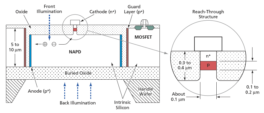
The advantages of the NAPD concept over prior photodetector and array concepts are attributable to the oxide embedding SOI structure and the nanoscale multiplication region. The electrically insulating property of the oxide embedding structure would prevent cross-talk among pixels. The nanoscale design of the multiplication region could be tailored to obtain unique avalanche properties. In contrast, (1) the pixels of a traditional APD array are all built on one common substrate, leading to severe cross-talk and (2) a traditional APD contains a relatively large multiplication region, within which electron avalanches are localized to a few small volumes. Efforts have been made to obtain uniformity in the multiplication regions of traditional APDs, but inasmuch as electron avalanches are very sensitive to the local electric-field fluctuations, it is difficult to obtain uniformity in large arrays of conventional APDs.
This work was done by Xinyu Zheng, Bedabrata Pain, and Thomas Cunningham of Caltech for NASA's Jet Propulsion Laboratory.
In accordance with Public Law 96-517, the contractor has elected to retain title to this invention. Inquiries concerning rights for its commercial use should be addressed to: Innovative Technology Assets Management
JPL
Mail Stop 202-233
4800 Oak Grove Drive
Pasadena, CA 91109-8099
(818) 354-2240
E-mail:
Refer to NPO-42276, volume and number of this NASA Tech Briefs issue, and the page number.
This Brief includes a Technical Support Package (TSP).
Nano-Multiplication-Region Avalanche Photodiodes and Arrays
(reference NPO-42276) is currently available for download from the TSP library.
Don't have an account?
Overview
The document is a Technical Support Package from NASA, specifically focusing on Nano-Multiplication-Region Avalanche Photodiodes (NAPDs) and their arrays, designated as NPO-42276. It outlines advancements in photon detection technology that aim to address significant challenges faced in low-light environments, particularly in applications requiring high dynamic range and sensitivity.
Traditional photon detection methods, such as Microchannel Plates (MCPs) and conventional avalanche photodiodes (APDs), have limitations. MCPs require high voltages, have a limited lifespan, and provide low dynamic range outputs. On the other hand, traditional APD arrays struggle with issues like crosstalk and after-pulsing effects, making them less competitive for single-photon detection. Charge-Coupled Devices (CCDs) and CMOS Active Pixel Sensors (APS) also face challenges due to readout noise, which hampers their ability to detect single photons effectively.
The document proposes a solution through structural innovations in avalanche photodiodes, resulting in NAPDs that possess several novel properties. These include very high quantum efficiency, low dark current, elimination of after-pulsing effects, complete removal of crosstalk, low power consumption, low voltage operation, and radiation hardness. Importantly, the self-quenching feature of these NAPDs allows for multiple counts per frame, significantly enhancing the dynamic range for photon counting.
The advancements presented in this document are positioned as competitive or even superior to existing technologies, making NAPDs a promising candidate for applications in various fields, including aerospace, where precise photon detection is crucial. The document emphasizes the potential of these innovations to revolutionize the way low-light detection is approached, paving the way for new scientific and commercial applications.
In summary, the Technical Support Package provides a comprehensive overview of the development and capabilities of Nano-Multiplication-Region Avalanche Photodiodes, highlighting their advantages over traditional methods and their potential impact on future technologies. It serves as a resource for understanding the ongoing research and technological advancements at NASA's Jet Propulsion Laboratory, aimed at enhancing photon detection capabilities in challenging environments.