
A complementary metal oxide/semiconductor (CMOS) integrated-circuit video image detector of the active-pixel-sensor (APS) type has been designed to implement programmable multiresolution output (through summing of outputs from selected groups of neighboring pixels) in a low-power, high-speed, low-noise differential column-readout scheme. This scheme increases (relative to CMOS APS devices of older designs) the signal-to-noise ratios achievable under low illumination.
Summing of signals from neighboring pixels, also called "pixel binning," amounts to trading away spatial resolution to increase sensitivity or decrease noise. This concept was described in "Active-Pixel Image Sensors With Programmable Resolution" (NPO-19510), NASA Tech Briefs, Vol. 20, No. 5 (May 1996), page 26. Pixel binning was implemented previously in a CMOS APS designed for frame-transfer operation. That CMOS APS proved to be susceptible to pickup of extraneous noise and to high residual fixed pattern noise (FPN) due to the use of a single-ended column integrator circuit. Moreover, the pixel binning was implemented by use of a two-dimensional-array analog memory circuit that more than doubled the area of the APS integrated-circuit chip. The differential column-readout scheme of the present CMOS APS reduces both FPN and temporal circuit noise. This scheme also eliminates the need for a two-dimensional memory array, thereby facilitating the development of CMOS APS devices with greater numbers of pixels and higher speed of operation.
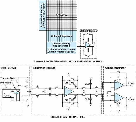
Like other typical CMOS APS devices, the present one comprises a two-dimensional array of photogates with active pixel and peripheral readout circuits. The selection of rows and columns for programming the dimensions and sequence of summation kernels is effected by use of externally generated control signals fed to row- and column-address decoders. The figure illustrates both the overall unique signal-processing architecture and the portion of the circuitry in the signal chain from one pixel to the output terminals.
To begin the pixel-summing process for a neighborhood of mby n pixels, each column integrator generates a sum of differential outputs from the pixels in the m selected contiguous rows in that column, in the following procedure: The signal (S) and reset (R) levels of each row are first sampled on the sample-and-hold capacitors CMS and CMR, respectively, as the column integrators are reset. Then the S and R levels are then differentially integrated on integrating capacitors CIS and CIR, respectively. The foregoing steps are repeated until the signals from all m rows in the neighborhood have been summed. The integrated levels are then sampled and held on the column memory capacitors CLS and CLR. A global integrator generates a differential output signal, one neighborhood at a time, by summing the signals from the memory capacitors of the n selected columns. The imager chip dissipates only 24 mW of power while running at 125 frames per second.
This work was done by Bedabrata Pain, Zhimin Zhou, and Eric Fossum of Caltech for NASA's Jet Propulsion Laboratory.
In accordance with Public Law 96-517, the contractor has elected to retain title to this invention. Inquiries concerning rights for its commercial use should be addressed to
Technology Reporting Office
JPL
Mail Stop 122-116
4800 Oak Grove Drive
Pasadena, CA 91109
(818) 354-2240
Refer to NPO-20344
This Brief includes a Technical Support Package (TSP).
Pixel-summing APS imager with differential column readout
(reference NPO20344) is currently available for download from the TSP library.
Don't have an account?
Overview
The document is a technical support package from NASA detailing the development of a Pixel-Summing APS (Active Pixel Sensor) Imager with Differential Column Readout, created by inventors Eric R. Fossum, Bedabrata Pain, and Zhimin Zhou at the Jet Propulsion Laboratory (JPL). The work was conducted under a contract with NASA and aims to address challenges in low-light imaging by enhancing the signal-to-noise ratio (S/N) of CMOS (Complementary Metal-Oxide-Semiconductor) imagers.
The primary motivation behind this innovation is the need for a low-power, high-performance imaging solution that can operate effectively in low illumination conditions. Traditional methods, such as pixel averaging and pixel binning, have been limited by issues like extraneous noise and high fixed pattern noise (FPN), which hinder their usability. The new architecture proposed in this document utilizes fully differential summing circuits and a single buffer stage, significantly improving performance by reducing FPN and temporal circuit noise.
One of the key advantages of this new imager design is its ability to eliminate the need for a 2-D analog memory array, which has previously complicated the implementation of large-format imagers. By operating from a single row buffer, the design allows for a more compact chip area, making it feasible to develop larger imaging systems suitable for various applications.
The document also discusses the novelty of the technology, emphasizing its improvements over prior art. It highlights the potential for practical realization in light-adaptive imaging applications, which is crucial for environments where lighting conditions can vary significantly.
Additionally, the document addresses the dissemination of this technology, indicating that it may be published in NASA Tech Briefs, a well-known publication that reaches a wide audience of potential customers and sponsors. The report underscores the importance of patent determination and inventor approval before publication.
In summary, this technical support package presents a significant advancement in imaging technology, focusing on a new CMOS APS imager that enhances image quality under low-light conditions while simplifying the architecture for large-format implementations. The work reflects JPL's commitment to innovation in aerospace and imaging technologies, with potential applications across various fields.