
Column-parallel analog-to-digital converters (ADCs) for imagers involve simultaneous operation of many ADCs. Single-slope ADCs are well adapted to this use because of their simplicity. Each ADC contains a comparator, comparing its input signal level to an increasing reference signal (ramp). When the ramp is equal to the input, the comparator triggers a latch that captures an encoded counter value (code). Knowing the captured code, the ramp value and hence the input signal are determined. In a column-parallel ADC, each column contains only the comparator and the latches; the ramp and code generation are shared.
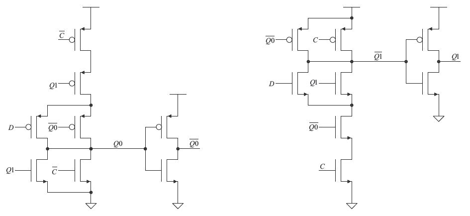
The circuit consists of two S-R (set-reset) latches, gated by the comparator. One is set by high data values and the other by low data values. The latches are cross-coupled so that the first one to set blocks the other. In order that the input data not need an inversion, which would consume power, the two latches are made in complementary polarity. This requires complementary gates from the comparator, instead of complementary data values, but the comparator only triggers once per conversion, and usually has complementary outputs to begin with.
An efficient CMOS (complementary metal oxide semiconductor) implementation of this circuit is shown in the figure, where C is the comparator output, D is the data (code), and Q0 and Q1 are the outputs indicating the capture of a zero or one value. The latch for Q0 has a negative-true set signal and output, and is implemented using OR-AND-INVERT logic, while the latch for Q1 uses positive-true signals and is implemented using AND-OR-INVERT logic. In this implementation, both latches are cleared when the comparator is reset. Two redundant transistors are removed from the reset side of each latch, making for a compact layout.
CMOS imagers with column-parallel ADCs have demonstrated high performance for remote sensing applications. With this latch circuit, the power consumption and noise can be further reduced. This innovation can be used in CMOS imagers and very-low-power electronics.
This work was done by Bruce R. Hancock of Caltech for NASA’s Jet Propulsion Laboratory.
In accordance with Public Law 96-517, the contractor has elected to retain title to this invention. Inquiries concerning rights for its commercial use should be addressed to:
Innovative Technology Assets Management
JPL
Mail Stop 321-123
4800 Oak Grove Drive
Pasadena, CA 91109-8099
E-mail: This email address is being protected from spambots. You need JavaScript enabled to view it.
NPO-48007
This Brief includes a Technical Support Package (TSP).

Minimal Power Latch for Single-Slope ADCs
(reference NPO-48007) is currently available for download from the TSP library.
Don't have an account?
Overview
The document titled "Minimal Power Latch for Single-Slope ADCs" discusses advancements in single-slope Analog-to-Digital Converters (ADCs), particularly their application in column-parallel digitization for image sensors. Authored by Bruce Hancock from NASA's Jet Propulsion Laboratory, the document outlines the benefits of single-slope ADCs, which include simplicity, excellent differential non-linearity (DNL), and good integral non-linearity (INL) when designed with a shared ramp generator. This shared architecture allows for automatic gain matching across multiple columns, making it particularly effective for high-density image sensor applications.
The core of the document focuses on a latch circuit designed to capture code values at the moment the ramp voltage crosses the input voltage, as indicated by a comparator. The design emphasizes the importance of using Gray code to represent the count, which helps prevent errors during code transitions, especially when using continuous-time comparators. The latch circuit is noted for its minimal power consumption, only drawing power when capturing data, which is crucial for energy-efficient designs.
The document also addresses potential issues with latch stability. It highlights that without positive feedback, latches may not settle into stable states, leading to mid-supply voltages that can cause excessive current flow through inverters. This is counterproductive to the goal of low power consumption. The proposed design actively clears latches when the comparator resets, ensuring that only one latch is set at any time, which enhances reliability and performance.
Illustrations in the document depict the implementation of the minimal power latch using complex logic gates and provide an efficient layout for the circuit. The design is compact and efficient, making it suitable for integration into larger systems.
Overall, the document serves as a technical support package that not only details the design and operation of the minimal power latch but also emphasizes its significance in advancing ADC technology for aerospace and other applications. It is a valuable resource for understanding the intersection of innovative technology and practical applications in the field of digital electronics.