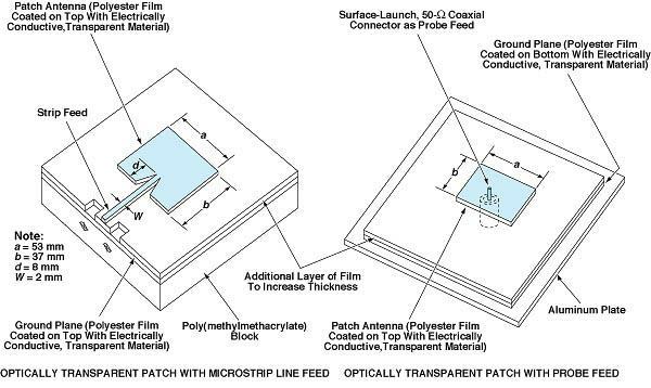
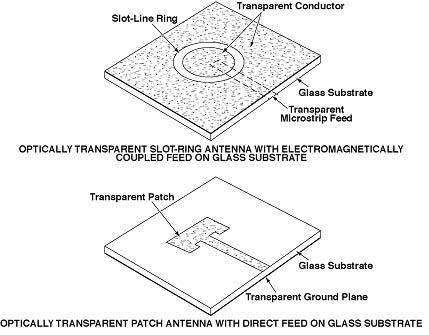
Optically transparent patch antennas have been invented for use in communication systems at frequencies of the order of a few gigahertz. These antennas can be mounted on windows of buildings and vehicles, on computer video monitors, on solar photovoltaic panels, and on other convenient supports; this is an advantage in situations in which the reuse of such supports for radio communication is dictated by a lack of room for adding separate antenna-supporting structures. Another advantage of the optically transparent patch antennas is that they weigh less than conventional antennas do.

An optically transparent patch antenna can be made from an optically transparent, electrically conductive film deposited on one face of a polyester film or a glass substrate; e.g., AgHT, or equivalent. In the case of a polyester film (see Figure 1), the deposited layer has a surface resistance of 6 to 10 ohms per square. The patch and its feed strip can be formed simply by cutting the coated film in the required pattern.
Typically, the polyester film is 0.0075 in. (0.19 mm) thick and is supported over a ground plane by an intervening nonconductive transparent film 0.0035 in. (0.089 mm) thick. Thus, the total thickness of dielectric material supporting the antenna patch is 0.011 in. (0.28 mm). The purpose of increasing the dielectric thickness by use of the intervening film is to increase the antenna bandwidth. Of course the fabrication of such an antenna on polyester film offers the advantage that the antenna can be bent to conform to a curved support.

Figure 2 presents examples of optically transparent patch antennas on glass substrates. Typically, a glass substrate is about 0.0115 in. (0.292 mm) thick and the deposited conductive film has a surface resistance of about 2.8 ohms per square. Whereas a polyester film must be cut to the required pattern, the conductive film on a glass substrate is patterned by depositing the conductive material through the open areas of a photoresist mask.
In tests, prototype optically transparent patch antennas like those shown in Figures 1 and 2 were found to exhibit radiation patterns, return losses, and input impedances similar to those of conventional patch antennas made from copper conductors. The observed radiation patterns are considered to be good for wireless communications, and the input impedances are well matched to the practical and commonly sought value of 50 ohms.
This work was done by Richard Q. Lee of Glenn Research Center and Rainee N. Simons of NYMA, Inc. For further information, access the Technical Support Package (TSP) free on-line at www.nasatech.com under the Electronic Components and Systems category.
Inquiries concerning rights for the commercial use of this invention should be addressed to
NASA Glenn Research Center
Commercial Technology Office
Attn: Steve Fedor
Mail Stop 4 – 8
21000 Brookpark Road
Cleveland
Ohio 44135.
Refer to LEW-16574.

