
A superconducting hot-electron bolometer has been built and tested as a prototype of high-sensitivity, rapid-response detectors of submillimeter-wavelength radiation. There are diverse potential applications for such detectors, a few examples being submillimeter spectroscopy for scientific research; detection of leaking gases; detection of explosive, chemical, and biological weapons; and medical imaging.
For this or any bolometer, a useful figure of merit that one seeks to minimize is (NEP)τ1/2, where NEP denotes the noise-equivalent power (NEP) and τ the response time. This figure of merit depends primarily on the heat capacity and, for a given heat capacity, is approximately invariant. As a consequence of this approximate invariance, in designing a device having a given heat capacity to be more sensitive (to have lower NEP), one must accept longer response time (slower response) or, conversely, in designing it to respond faster, one must accept lower sensitivity. Hence, further, in order to increase both the speed of response and the sensitivity, one must make the device very small in order to make its heat capacity very small; this is the approach followed in developing the present device.
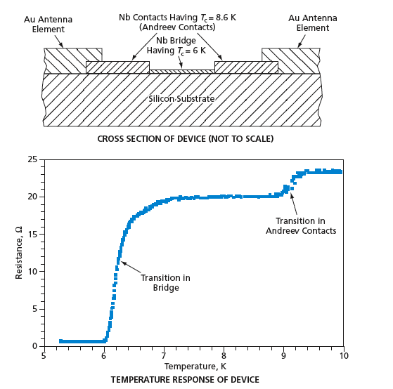
In the present device, the superconducting bridge having the Tc of 6 K is a thin film of niobium on a silicon substrate (see figure). This film is ≈1 μm wide, ≈1 μm long, and between 10 and 25 nm thick. A detector so small could lose some sensitivity if thermal energy were allowed to diffuse rapidly from the bridge into the contacts at the ends of the bridge. To minimize such diffusion, the contacts at the ends of the bridge are made from a 150-nm-thick niobium film that has a higher Tc(8.6 K). The interfaces between the bridge and the contacts constitute an energy barrier of sorts where Andreev reflection occurs. As a result, the sensitivity of the device depends primarily on thermal coupling between electrons and the crystal lattice in the Nb bridge. For this device, (NEP) = 2 × 10–14 W/Hz1/2 and the response time is about 0.5 ns.
In order to obtain high quantum efficiency, a planar spiral gold antenna is connected to the niobium contacts. The antenna enables detection of radiation throughout the frequency range from about 100 GHz to several terahertz. In operation, radiation is incident from the underside of the silicon substrate, and an antireflection-coated silicon lens (not shown in the figure) glued to the underside of the substrate focuses the radiation on the bridge (this arrangement is appropriate because silicon is transparent at submillimeter wavelengths).
This work was done by Boris Karasik, William McGrath, and Henry Leduc of Caltech for NASA’s Jet Propulsion Laboratory. NPO-43619
This Brief includes a Technical Support Package (TSP).
Superconducting Hot-Electron Submillimeter-Wave Detector
(reference NPO-43619) is currently available for download from the TSP library.
Don't have an account?
Overview
The document presents a technical overview of a fast and sensitive hot-electron Nb direct detector designed for submillimeter (submm) imaging and spectroscopy, developed by researchers at NASA's Jet Propulsion Laboratory (JPL). The primary objective of this research is to create a detector suitable for high-background applications in spectroscopy and imaging, particularly in the context of astrophysical studies.
The detector utilizes a phonon-cooled niobium (Nb) hot-electron bolometer with Andreev contacts, which effectively block the outdiffusion of hot electrons from the device. This design allows the detector to achieve a very low noise equivalent power (NEP) of approximately 1 fW/Hz^1/2, making it background-limited at 300 K with an optical bandwidth of 1-2 THz. The device operates at high speeds, with an effective output bandwidth of around 300 MHz, and is fabricated using thin film techniques on silicon, enabling integration into compact arrays.
The document details the construction of the detector, which consists of submicron-sized devices made from a magnetron-sputtered Nb film, featuring 150 nm Nb Andreev contacts and an antenna for signal reception. The superconducting transition temperatures of the materials used are highlighted, with the device operating in a resistive state at lower temperatures compared to the contacts, which helps maintain thermal stability and performance.
Applications of this detector technology are broad, including submm lab spectroscopy for dynamic measurements of water line resonances, which are crucial for astrophysical models. Potential space applications include fast-scan Fourier spectroscopy of planetary atmospheres and comets. Additionally, the technology has implications for non-space applications such as port security imaging, biological and chemical weapon detection, and gas leak detection.
Despite its advantages in sensitivity and speed over room-temperature detectors, the requirement for active cooling presents challenges for broader application. The document emphasizes that the availability of lightweight and compact mechanical cryocoolers will be a critical factor in the wider adoption of this detector technology.
Overall, this research represents a significant advancement in detector technology, with the potential to enhance our understanding of various scientific fields through improved imaging and spectroscopy capabilities.