
Paper-Thin Optical Lens

Paper-thin optical lenses simple enough to mass produce like microchips could enable a new generation of compact optical devices. A team with researchers at the University of Tokyo and JSR Corp. fabricated and tested flat lenses called Fresnel zone plates (FZPs) but did so for the first time using only common semiconductor manufacturing equipment, the i-line stepper, for the first time. These flat lenses currently lack the efficiency of in-production lenses but have the potential to reshape optics for industries ranging from astronomy to healthcare and consumer electronics. Flat lenses, such as metalenses, exist, but they come with hefty price tags and a high degree of complexity, and only a small number of devices are available. The researchers used a simple and mass-producible method for FZPs using a common semiconductor lithography system, or stepper. FZPs have become a good candidate to improve optical devices where space is critical.
Contact: Kuniaki Konishi
+81 3-3812-2111
This email address is being protected from spambots. You need JavaScript enabled to view it.
Compact Cooling Tech
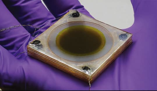
Materials scientists at the University of California, Los Angeles, have developed a compact cooling technology that can pump away heat continuously using layers of flexing thin films. The design is based on the electrocaloric effect, in which an electric field causes a temporary change in a material’s temperature. The experimental material is composed of a circular stack of six thin polymer films, just under an inch in diameter and one-quarter of an inch thick for the entire stack. Each layer is coated with carbon nanotubes on both sides. The resulting material is ferroelectric, which means it changes shape when an electric field is applied. In lab experiments, the researchers found that the prototype could lower ambient temperatures of its immediate surroundings by 16 °F continuously and up to 25 °F at the source of the heat after about 30 seconds. Such a cooling mechanism would be most ideal for next-generation wearables that can keep us cool under strenuous conditions.
Contact: Matthew Chin
310-825-4321
This email address is being protected from spambots. You need JavaScript enabled to view it.
Stackable 3D Chip

MIT engineers have created a multilayered chip design that doesn’t require any silicon wafer substrates and works at temperatures low enough to preserve the underlying layer’s circuitry. The method enables engineers to build high-performance transistors and memory and logic elements on any random crystalline surface — not just on the bulky crystal scaffold of silicon wafers. Without these thick silicon substrates, multiple semiconducting layers can be in more direct contact, leading to better and faster communication and computation between layers, the researchers say. The researchers envision that the method could be used to build AI hardware, in the form of stacked chips for laptops or wearable devices, that would be as fast and powerful as today’s supercomputers and could store huge amounts of data on par with physical data centers.