
Two-dimensional materials, which are only a few atoms thick, can exhibit some incredible properties, such as the ability to carry electric charge extremely efficiently, which could boost the performance of next-generation electronic devices.
But integrating 2D materials into devices and systems like computer chips is notoriously difficult. These ultrathin structures can be damaged by conventional fabrication techniques, which often rely on the use of chemicals, high temperatures, or destructive processes like etching.
To overcome this challenge, researchers from MIT and elsewhere have developed a new technique to integrate 2D materials into devices in a single step while keeping the surfaces of the materials and the resulting interfaces pristine and free from defects.
Their method relies on engineering surface forces available at the nanoscale to allow the 2D material to be physically stacked onto other prebuilt device layers. Because the 2D material remains undamaged, the researchers can take full advantage of its unique optical and electrical properties.
They used this approach to fabricate arrays of 2D transistors that achieved new functionalities compared to devices produced using conventional fabrication techniques. Their method, which is versatile enough to be used with many materials, could have diverse applications in high-performance computing, sensing, and flexible electronics.
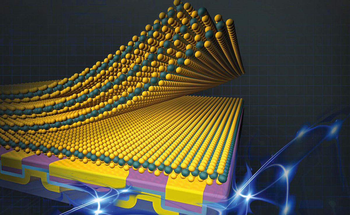
Core to unlocking these new functionalities is the ability to form clean interfaces, held together by special forces that exist between all matter, called van der Waals forces.
However, such van der Waals integration of materials into fully functional devices is not always easy, said Farnaz Niroui, Assistant Professor of Electrical Engineering and Computer Science (EECS), a member of the Research Laboratory of Electronics (RLE), and senior author of a new paper describing the work.
“Van der Waals integration has a fundamental limit,” she explained. “Since these forces depend on the intrinsic properties of the materials, they cannot be readily tuned. As a result, there are some materials that cannot be directly integrated with each other using their van der Waals interactions alone. We have come up with a platform to address this limit to help make van der Waals integration more versatile, to promote the development of 2D-materials-based devices with new and improved functionalities.”
To make electronic devices, they form a hybrid surface of metals and insulators on a carrier substrate. This surface is then peeled off and flipped over to reveal a completely smooth top surface that contains the building blocks of the desired device.
This smoothness is important, since gaps between the surface and 2D material can hamper van der Waals interactions. Then, the researchers prepare the 2D material separately, in a completely clean environment, and bring it into direct contact with the prepared device stack.
This single-step process keeps the 2D material interface completely clean, which enables the material to reach its fundamental limits of performance without being held back by defects or contamination.
And because the surfaces also remain pristine, researchers can engineer the surface of the 2D material to form features or connections to other components. For example, they used this technique to create p-type transistors, which are generally challenging to make with 2D materials. Their transistors have improved on previous studies and can provide a platform toward studying and achieving the performance needed for practical electronics.
In the future, the researchers want to build on this platform to enable integration of a diverse library of 2D materials to study their intrinsic properties without the influence of processing damage and develop new device platforms that leverage these superior functionalities.
For more information, contact Abby Abazorius at