

In order to continue improving microprocessor technology, semiconductor manufacturers have turned to so-called “heterogeneous computing.” This shift is necessary because it is no longer feasible to boost computing performance just by further shrinking transistors or increasing core counts on a single die.

Heterogeneous computing involves packaging different types of integrated circuits (such as CPUs, GPUs, and memory) together to function essentially like a single chip. There are many different embodiments of these “advanced packaging” methods. But they all involve assembling multiple ICs on to compact, high-density substrates. And these substrates are significantly thinner and more delicate than those used in traditional electronics packaging and incorporate finer geometries as well.
This is where lasers, and specifically diode pumped solid state (DPSS) lasers, play a critical role. DPSS laser-based cutting and drilling techniques are uniquely capable of delivering the precision, cut quality, and material versatility required for fabricating advanced packaging substrates. They enable the formation of microvias and trenches, and singulate packaged IC dies, with minimal thermal damage in ways that can’t be achieved with mechanical techniques or even fiberlasers, commonly used for a variety of material processing tasks. Fiber lasers, which have been so successful in many other industrial applications, tend to be used for less demanding cuts or metal processing.
DPSS lasers are also available with many different operational modes and wavelengths. The main differentiator is typically pulse width – which is usually either nanosecond or ultrashort (picosecond or femtosecond). And, DPSS lasers are available at wavelengths in the infrared (around 1 μm), green (around 530 nm), and UV (around 355 nm), providing the versatility required for a wide range of semiconductor advanced packaging types.
To evaluate these lasers in real-world singulation applications, MKS Spectra-Physics® applications engineers conducted a series of cutting tests on substrates commonly used for system-in-package (SiP) – a popular advanced packaging method. The objective was to assess overall effectiveness and to quantify differences in cut quality and system performance between nanosecond pulse lasers and ultrashort pulse (USP) lasers. These results should provide useful guidance for those selecting a laser for advanced packaging applications.
Nanosecond Laser Singulation

The nanosecond pulse laser used for testing was a MKS Spectra-Physics Talon® GR70, which provides 70 W of output at 532 nm (green). It was used to make through cuts in SiP material comprised of thin FR4 with embedded copper traces and solder mask layers on both sides. Total thickness of this material was 250 μm, 150 μm of which was the FR4 board, with the remaining 100 μm being the polymeric solder masks.
The laser was focused down to about 16 μm on the material surface and operated at a repetition rate of 450 kHz. A galvanometer scanner was used to move the beam at 6 m/s — a relatively high speed which allows for heat dissipation and therefore minimal heat-affected zone (HAZ) formation. Multiple passes were used to achieve a through cut, and the net cutting speed was 200 mm/s.
Optical microscope photos (Figure 1) show entry and exit surfaces of the cut, plus a subsurface area where the cutting path crossed over a buried copper trace. Both the entry and exit surfaces are cleanly cut with little evidence of HAZ, and minimal surface residue was generated. In addition, the presence of the copper trace did not significantly affect the cutting process.
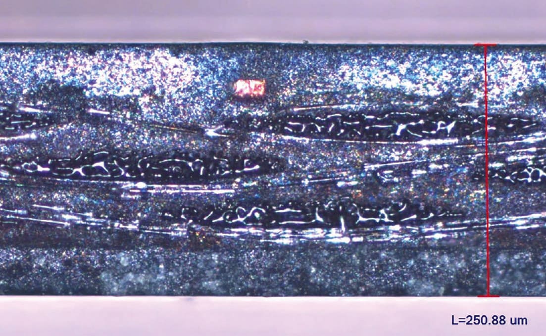
The image in Figure 2 is a cross-sectional view of the cut sidewall. This shows good cut quality, a small HAZ, and limited carbonization. The individual fibers in the FR4 layer are clearly discernible, with melting limited to the cut fiber end faces oriented outward from the sidewall.
Most importantly, this image shows no delamination of layers. Plus, this image confirms a good quality Cu trace line cut that did not suffer detrimental thermal effects, such as outflow of molten copper or delamination at the FR4/ solder mask boundary, where the trace is located.
In general, the cut quality produced by this green nanosecond laser is quite good, and it achieves high cutting speeds. But close inspection of the sidewall does reveal minor melting of glass fibers, the significance of which will depend on specific application requirements.
USP Laser Singulation
An MKS Spectra-Physics IceFyre® GR50 operating at 532 nm was used for the USP laser cutting tests. But because a USP laser is expected to be reserved for more demanding and delicate processing tasks, this testing was performed on a thinner substrate. Specifically, this was a 200 μm thick FR4 substrate having polymer solder mask protective layers on both sides, plus intermittent embedded copper trace lines layered along the intended cutting path. The FR4 itself was only about 100 μm thick.
Initial tests were made with the laser operating at 40 W and a repetition rate of 400 kHz. Multi-pass scanning was again employed so that the scanning speed of 4 m/s yielded an effective cutting speed of 57 mm/s.
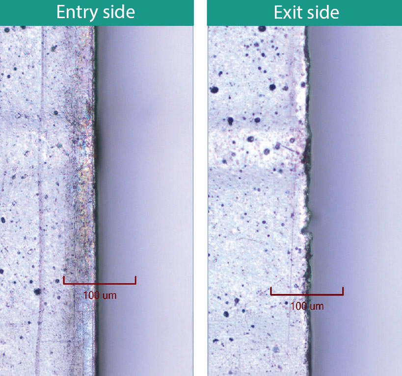
Microscope photographs (Figure 3) show the entry surface which includes a cut through a copper trace. The surface quality is excellent overall, with better cut edge quality and significantly less debris than with the nanosecond laser cut.
However, it appears that excess heating around the copper layer caused slight erosion of the polymer/FR4 material around it. This resulted in a minor protrusion of the copper from the sidewall. (Note that the laser-cut feature is shown here without any post-processing cleaning, in contrast to the previous result displayed for the ns pulse laser.)
Further work showed that results could be improved by reducing the laser power 50 percent (20 W), along with other parameter adjustments. The scanning speed was increased to 6 m/s, resulting in a net cutting speed of 38 mm/s.
The microscope photos (Figure 4) show the improved cut quality obtained at 50 percent power. There is an even greater reduction in debris, and once again, there was no post-process cleaning. Both the HAZ around the copper trace and the protrusion of the copper are absent here.
It’s also worth noting that working at 50 percent power provides a significant operational advantage. Specifically, the laser can be operated at full power, but in a two-beam split configuration, with each beam entering separate processing stations and working simultaneously. This doubles the overall system cutting speed to 2×38 = 76 mm/s, which is 33 percent greater than the single full-power beam.
Conclusions
Based on an understanding of the laser/material interaction and the test results presented here, it should be clear that DPSS lasers have significant advantages processing these semiconductor advanced packages; however, there is no single “best” DPSS laser for advanced packaging. The choice depends on balancing precision, throughput, and cost.
Reducing pulse width clearly improves feature quality but often at the expense of processing speed. However, if the improved quality eliminates subsequent cleaning steps, overall throughput may not suffer.
This is not surprising. In general terms, the photothermal material removal mechanism characteristic of nanosecond lasers delivers higher material removal rates but produces a larger HAZ. USP lasers, which operate at least partially through more direct photoablation, typically offer lower material removal rates but minimize or virtually eliminate the HAZ. Shorter wavelengths are also well-established as producing smaller features and better energy coupling to more material types.
Beyond quality versus speed tradeoffs, practical factors matter. USP lasers are more expensive and complex than nanosecond lasers. Similarly, UV lasers cost more and offer lower output power than their visible and IR counterparts. This can lead to higher capital cost and lower throughput. For many SiP applications, nanosecond green lasers offer the best compromise between cost, precision, and productivity.
In conclusion, DPSS lasers are a critical enabling technology for meeting the precision materials processing demands of advanced packaging. Both nanosecond and USP lasers can achieve excellent results, but the right choice depends on specific requirements. Success in a given application often depends on partnering with a supplier that offers a full range of laser technologies, from nanosecond to USP, and from IR to UV, along with the expertise to apply them effectively.
This article was written by Jim Bovatsek, Senior Manager of Application Engineering, MKS Spectra‑Physics (Milpitas, CA). For more information, email Jim at