
A proposed visible-light imaging spectrometer on a chip would be based on the concept of a heterostructure comprising multiple layers of silicon-based photodetectors interspersed with long-wavelength-pass optical filters. In a typical application, this heterostructure would be replicated in each pixel of an image-detecting integrated circuit of the active-pixel-sensor type (see figure).
The design of the heterostructure would exploit the fact that within the visible portion of the spectrum, the characteristic depth of penetration of photons increases with wavelength. Proceeding from the front toward the back, each successive long-wavelength-pass filter would have a longer cutoff wavelength, and each successive photodetector would be made thicker to enable it to absorb a greater proportion of incident longer-wavelength photons.
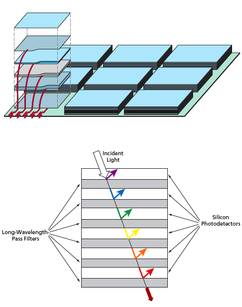
Incident light would pass through the first photodetector and encounter the first filter, which would reflect light having wavelengths shorter than its cutoff wavelength and pass light of longer wavelengths. A large portion of the incident and reflected shorter-wavelength light would be absorbed in the first photodetector.
The light that had passed through the first photodetector/filter pair of layers would pass through the second photodetector and encounter the second filter, which would reflect light having wavelengths shorter than its cutoff wavelength while passing light of longer wavelengths. Thus, most of the light reflected by the second filter would lie in the wavelength band between the cutoff wavelengths of the first and second filters. Thus, further, most of the light absorbed in the second photodetector would lie in this wavelength band. In a similar manner, each successive photodetector would detect, predominantly, light in a successively longer wavelength band bounded by the shorter cutoff wavelength of the preceding filter and the longer cutoff wavelength of the following filter.
This work was done by Yu Wang, Bedabrata Pain, Thomas Cunningham, and Xinyu Zheng of Caltech for NASA's Jet Propulsion Laboratory. For more information, download the Technical Support Package (free white paper) at www.techbriefs.com/tsp under the Semiconductors & ICs category. NPO-41125
This Brief includes a Technical Support Package (TSP).
Imaging Spectrometer on a Chip
(reference NPO-41125) is currently available for download from the TSP library.
Don't have an account?
Overview
The document presents a technical support package from NASA's Jet Propulsion Laboratory (JPL) detailing an innovative "Imaging Spectrometer on a Chip." This technology addresses the limitations of traditional spectrometers, which are typically heavy and cumbersome, often weighing several kilograms. The proposed solution is a lightweight, on-chip spectrometer that utilizes a vertical hetero structure of long pass optical filters and silicon films, enabling efficient multi-wavelength imaging.
The core principle behind this technology is the varying penetration depth of photons in silicon, which is dependent on their wavelength. Shorter wavelength photons are absorbed in a thin surface layer, while longer wavelengths can penetrate deeper before being absorbed. This characteristic allows for the design of a spectrometer that can effectively separate and analyze different wavelength bands using longpass optical filters. Each filter has a sharp cutoff wavelength, reflecting shorter wavelengths and transmitting longer ones, which facilitates precise photon absorption and minimizes interference from longer wavelength bands.
The document outlines the structure of the proposed on-chip spectrometer, which consists of multiple silicon layers of varying thicknesses paired with longpass filters. This configuration allows for the creation of a six-band spectrometer, capable of distinguishing between different wavelengths with high efficiency. The design aims to eliminate the photon absorption tails that can complicate spectral analysis, thereby enhancing the accuracy of the measurements.
Figures included in the document illustrate the technology's principles, including the transmission characteristics of longpass filters and the photon absorption profiles of silicon layers. The innovative design is positioned to support NASA's current and future missions related to multi-spectrum and hyper-spectrum imaging, which are crucial for remote sensing and in situ analysis of various environments.
Overall, the "Imaging Spectrometer on a Chip" represents a significant advancement in spectrometry technology, promising to improve the efficiency and effectiveness of imaging systems used in aerospace applications. This development aligns with NASA's goals of enhancing scientific exploration capabilities while reducing the weight and complexity of imaging instruments.