54
-1
0
30
Briefs: Sensors/Data Acquisition
A new study from NC State University combines three-dimensional embroidery techniques with machine learning to create a fabric-based sensor that can control electronic devices through touch. Read on to learn more.

Briefs: Semiconductors & ICs
Optics researchers in the Harvard John A. Paulson School of Engineering and Applied Sciences created specially designed metasurfaces — flat devices etched with nanoscale light-manipulating patterns — to act as ultra-thin upgrades for quantum-optical chips and setups. Read on to learn more.

Briefs: Information Technology
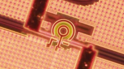
Cornell researchers have developed a low-power microchip they call a “microwave brain,” the first processor to compute on both ultrafast data signals and wireless communication signals by harnessing the physics of microwaves. Read on to learn more about it.

Briefs: Robotics, Automation & Control
Researchers at Fuzhou University in China created a machine vision sensor that uses quantum dots to adapt to extreme changes in light far faster than the human eye can — in about 40 seconds — by mimicking eyes’ key behaviors. Their results could be a game changer for robotic vision and autonomous vehicle safety. Read on to learn more.

Briefs: Sensors/Data Acquisition
Maksym Kovalenko and his team have proposed a novel solution that allows them to utilize every photon of light for color recognition. For nearly a decade, they have been researching perovskite-based image sensors. In a new study published in Nature, they show that their new technology works. Read on to learn more.

Briefs: Electronics & Computers
University of California San Diego and CEA-Leti scientists have developed a ground-breaking piezoelectric-based DC-DC converter that unifies all power switches onto a single chip to increase power density. Read on to learn more about this new power topology, which extends beyond existing topologies and blends the advantages of piezoelectric converters with capacitive-based DC-DC converters.

Briefs: Sensors/Data Acquisition
Engineers at MIT, Nanyang Technological University, and several companies have developed a compact and inexpensive technology for detecting and measuring lead concentrations in water, potentially enabling a significant advance in tackling this persistent global health issue. Read on to learn more.

Briefs: Photonics/Optics
AI systems like ChatGPT are notorious for being power-hungry. To tackle this challenge, a team from the Centre for Optics, Photonics and Lasers has come up with an optical chip that can transfer massive amounts of data at ultra-high speed. As thin as a strand of hair, this technology offers unrivaled energy efficiency. Read on to learn more.
Briefs: Semiconductors & ICs
Researchers have invented a new type of tunable semiconductor laser that combines the best attributes of today’s most advanced laser products, demonstrating smooth, reliable, wide-range wavelength tuning in a simple, chip-sized design. Read on to learn more about it.

Briefs: Software
A research team led by scientists at Lawrence Berkeley National Laboratory (Berkeley Lab) has developed a new fabrication technique that could improve noise robustness in superconducting qubits, a key technology for enabling large-scale quantum computers. Read on to learn more.

Briefs: Semiconductors & ICs
A new computer vision technique developed by MIT engineers significantly speeds up the characterization of newly synthesized electronic materials. The technique automatically analyzes images of printed semiconducting samples and quickly estimates two key electronic properties for each sample. Read on to learn more.

Briefs: Sensors/Data Acquisition
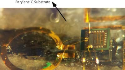
An invention that uses microchip technology in implantable devices and other wearable products such as smart watches can be used to improve biomedical devices including those used to monitor people with glaucoma and heart disease. Read on to learn more.
Briefs: Electronics & Computers
Researchers have designed and synthesized a unique material with controllable capabilities that make it promising for future electronics including cellphones and computers. Read on to learn more.

Briefs: RF & Microwave Electronics
Artificial intelligence systems promise transformative advancements, yet their growth has been limited by energy inefficiencies and bottlenecks in data transfer. Researchers at Columbia Engineering have unveiled a groundbreaking solution: a 3D photonic-electronic platform that achieves unprecedented energy efficiency and bandwidth density, paving the way for next-generation AI hardware. Read on to learn more.

Briefs: Data Acquisition
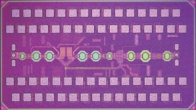
Researchers have developed a photonic chip-based traveling wave parametric amplifier that achieves ultra-broadband signal amplification in an unprecedentedly compact form. Read on to learn more about it.

Briefs: Semiconductors & ICs
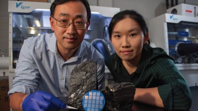
A joint research effort led by the University of Illinois Urbana-Champaign has shown how coal can play a vital role in next-generation electronic devices. Read on to learn more about it.
Briefs: Semiconductors & ICs
The mass production of conventional silicon chips relies on a successful business model with large “semiconductor fabrication plants” or “foundries.” New research by KU Leuven and imec shows that this “foundry” model can also be applied to the field of flexible, thin-film electronics. Read on to learn more.

Briefs: Materials
A Duke University team's approach takes a metallic nanotube, which always lets current through, and transforms it into a semiconducting form that can be switched on and off. Read on to learn more.

Briefs: Manufacturing & Prototyping
Manufacturing More Efficient Spintronics Devices
Researchers have developed a breakthrough process for making spintronic devices that has the potential to become the new industry standard for semiconductors chips that make up computers, smartphones, and many other electronics. The new process will allow for faster, more efficient spintronics devices that can be scaled down smaller than ever before. Read on to learn more about it.
Briefs: Green Design & Manufacturing
Researchers have developed a strategy to design luminescent polymers with high light-emitting efficiencies from the start that are both biodegradable and recyclable. Read on to learn more.

Briefs: Photonics/Optics
A Bristol-led team of physicists has found a way to operate mass manufacturable photonic sensors at the quantum limit. This breakthrough paves the way for practical applications such as monitoring greenhouse gases and cancer detection. Read on to learn more.
Briefs: Photonics/Optics
Researchers have created visible lasers of very pure colors from near-ultraviolet to near-infrared that fit on a fingertip. The colors of the lasers can be precisely tuned and extremely fast — up to 267 petahertz per second, which is critical for applications such as quantum optics. Read on to learn more.

Briefs: Photonics/Optics
Researchers have designed a spiral ladder-inspired tool that allows precision control of light direction and polarization to control the direction of the emitted beam and the polarization of the light, while using a precisely engineered resonance of the structure. Read on to learn more.

Briefs: Software
Researchers have successfully developed a wide-bandwidth, low-polarization semiconductor optical amplifier based on tensile-strained quantum wells. The study, published in the journal Sensors, presents a significant advancement in optical communication technology, addressing the growing demand for higher bandwidth and lower polarization sensitivity. Read on to learn more.

Briefs: Electronics & Computers
Researchers from MIT and elsewhere have developed a new technique to integrate 2D materials into devices in a single step while keeping the surfaces of the materials and the resulting interfaces pristine and free from defects. Read on to learn more.

Briefs: Software
A new approach uses commercial chip fab materials and techniques to fabricate specialized transistors to serve as the building block of the timing device. Read on to learn more.

Briefs: Materials
It's time to rethink battery technology. Compared to other existing or developing technologies, a new lithium metal-based solid-state battery brings some significant advantages: It can be charged and discharged within one minute, lasts about 10 times as long as a Li-ion battery, and is insensitive to temperature fluctuations. Read on to learn more about it.
Briefs: Sensors/Data Acquisition
Researchers at the University of California, Davis, have developed a proof-of-concept sensor that may usher in a new era for millimeter wave radars. They call its design a “mission impossible” made possible. Read on to learn more.
Briefs: Materials
Researchers at Stanford have been working on skin-like, stretchable electronic devices for over a decade. Recently, they presented a new design and fabrication process for skin-like integrated circuits that are five times smaller and operate at one thousand times higher speeds than earlier versions. Read on to learn more about it.

Top Stories
 Blog: Lighting
A Stretchable OLED that Can Maintain Most of Its Luminescence
 Blog: Energy
Batteries that Can Withstand the Cold
 INSIDER: Energy
Advancing All-Solid-State Batteries
 Quiz: Energy
 Blog: Physical Sciences
 Blog: Materials
Webcasts
 Upcoming Webinars: Test & Measurement
From Spreadsheets to Insights: Fast Data Analysis Without Complex...
 Upcoming Webinars: Electronics & Computers
Cooling a New Generation of Aerospace and Defense Embedded...
 Upcoming Webinars: Test & Measurement
Beyond AI-Copy-Paste Engineering: Advanced AI-Integration Success...
 Upcoming Webinars: Automotive
Battery Abuse Testing: Pushing to Failure
 Upcoming Webinars: Internet of Things
A FREE Two-Day Event Dedicated to Connected Mobility
 Upcoming Webinars: Test & Measurement
Choosing the Right N-Port Strategy: Multiport VNAs vs. Switch...