Each passing year, machine vision is finding its way into applications that were not commercially feasible — and in some cases, impossible — prior to new software advances such as deep learning and related neural network processing techniques. Despite being some 50 years along the maturation curve, machine vision is just beginning to see its full potential as it heads toward the next industrial revolution, marked by increased machine-to-machine cooperation and machine-to-human collaboration.

The growth in machine vision adoption, prompted in large part by the convergence of advanced imaging analysis, robotics, machine learning, and related automation, is leading to creative, never-before-seen solutions, to unique challenges inside and outside the factory. As the “eyes” of the system, machine vision cameras will remain critical to the development of next-level solutions in a variety of growing global markets.
Sensor Type: CCD, CMOS, and More
Since global shutters came to complementary metal oxide semiconductor (CMOS) optical sensors, the market has long predicted the demise of the charge-coupled detector (CCD) due to advantages of CMOS. It has a cheaper manufacturing process, higher speed operation, and ability to integrate microprocessors, memory, and other standard electronic blocks on chip (e.g., Xilinx's Xinq, Intel Movidius, Max10, and Cyclone). But like so many predictions, each new year brings renewed — and mistaken — reports of CCD's demise.
CCD maintains a strong position in life sciences and related applications because of its ability to reduce the depth of the silicon layer on the back of the sensor (back-thin) for greater optical sensitivity, lack of fixed pattern noise, and lower noise floor. However, CMOS has taken over the majority of the machine vision market. CCD sensors still offer fewer dead pixels compared with standard CMOS chip yields and higher quantum efficiency/responsivity, which is important for near infrared (NIR), scientific, and life science applications. These include microscopy and endoscopy applications, where sensitivity is critical to acquiring useful images.
Other types of sensors include microbolometer and InGaAs sensors in IR/thermal vision applications — a common technique used to monitor assets based on operating temperature in forges, metal working, and related applications.
Resolution: Area Arrays, Line Scan
Every few years, optical sensor yields improve enough to reduce costs to where machine vision customers can jump from one resolution plateau to the next. This holds true whether we are talking area arrays or linear arrays, i.e., line scan cameras. In general, more resolution offers one of two benefits: either more pixels to help identify a defect in an image (e.g., smaller defects on shrinking wafer traces), or the ability to do more inspections in a given field of view (e.g., large wafer/flat-panel inspections) — especially as even “dumb” component cameras start to add user-set multiple regions of interest to their available feature offerings.

In 2018, the most common component camera went from 2 to 5 megapixels (MP). In the next couple of years, camera OEMs are predicting a jump to 10 MP as the standard size of a machine vision sensor array. This is achievable while still maintaining realistic pixel sizes of several microns square so that the most commonly available optics still have the ability to resolve light on individual pixels. This is unlike the massive sensor arrays in smart phones with cheap optics that cannot deliver on the true resolution promise of 12+ MP sensors with pixels of 1.4 μm. Conversely, some of the largest machine vision cameras today for the semiconductor industry offer 50 MP with 5-μm pitch pixels, providing massive resolutions at viable pixel sizes for standard camera optics.
Within the line scan segment, 8k array lengths are the new norm, up from 4k line scan. Thanks to the ability to build just one, or only a few, rows of pixels, line scan cameras are able to maintain large pixel sizes for light sensitivity more easily while still running at high readout speeds. In some cases, they use multiple “taps” to read out sections of a long linear array sensor and time domain integration (TDI) to bin multiple rows of pixels into a single pixel value. These techniques allow new cameras to keep up with increasing production line speeds. Insiders say the next linear array plateau is likely to be 15 to 16k linear arrays, which will place additional requirements on the optics to capture as much light as possible across the full sensor length.
The challenge of matching optics with larger sensor sizes sporting smaller pixels will continue into the future among both area and linear array sensor groups. Camera experts say 3-μm pixels is the line at which developing effective, cost-efficient, optics becomes problematic, if not practically impossible, using today's optical manufacturing technology.
Speed: Area Arrays, Line Scan
Higher speed, usually defined by a camera's frame rate, allows customers to inspect more products per minute and/or help to freeze the motion of fast-moving objects while limiting blur. This improves the machine vision system's ability to make an accurate automated decision or measurement.

Today, 200 fps speeds for area arrays and 70 kHz frame rates for 4k linear arrays are fairly common, with maximum frame rates two to three times above those levels. Luckily for the camera interfaces, few customers operate machine vision cameras at 100% of full frame rate. Instead, common applications acquire several images in a very short period of time and then send the data to the processing unit in a burst, easing the bandwidth requirements on imaging networks.
GigE Vision can accommodate the majority of applications and the frame rates and data transmission bandwidth requirements of the associated cameras. I/O specialists in imaging network applications, however, say they are seeing interest in 2.5 Gpbs GigE Vision over NBASE-T as an intermediate step towards 10GigE. Today, consumer markets have yet to adopt 10GigE as the default port in desktops and laptops due to cost, power consumption, and thermal design challenges.
In general, machine vision camera OEMs of area and linear arrays believe that while special cases will always exist in which customers want cameras that run at higher speeds, most applications are adequately served by today's off-the-shelf camera offerings. If a bottleneck exists for a given application, it's usually in the network at this point. This necessitates a move toward a frame grabber–based protocol such as Camera Link High Speed, which has a higher throughput than standard GigE Vision and USB3 Vision.
Color Cameras and Lighting
Machine vision integrators estimate that despite regular growth of color machine vision cameras, 90% of machine vision applications are solved by a monochrome camera. Traditionally, the reason has been cost, as color cameras are more expensive than monochrome cameras with the same resolution. The cost-per pixel issue becomes more pronounced if the color camera uses the common Bayer filter, which reduces the camera's resolution to one-third of the original resolution.
For the most accurate color representation, 3CCD cameras have been the standard. These cameras use a prism to separate the colors, rather than filters applied directly to a single array. In this case, each sensor acquires one color channel, and the three separate images are combined in software to produce a more realistic representation of the object than is achievable by using Bayer filters. Additionally, this more costly approach does not come with a resolution penalty. For the most accurate print inspection applications, for example, prism-based chip line scan cameras have been the gold standard for years. This has been due to the accuracy of the color representation, the ability to limit spectral overlap between channels, and improved spatial alignment between color channels.
In the past year, the machine vision camera market has seen the first line scan camera to offer different polarization filters applied to different rows, a useful feature for flat-panel display inspection. Camera OEMs expect this trend toward multichannel, customized filtering to continue.
Lighting is also taking a more active role in machine vision solutions in general, but in color applications in particular. Cameras with multiple exposures and regions of interest can perform multiple inspections, many of which may require different illumination techniques. Some camera OEMs are using single-sensor cameras and time domain rather than optical filtering to separate color channels. This results in multispectral solutions with lower throughput and lower cost but requires more complex illumination sources and controls.
The most prevalent applications for machine vision cameras still use visible light. Certain applications, however, utilize less popular lighting methods, such as x-ray, ultraviolet (UV), near infrared (NIR), shortwave infrared (SWIR), and long-wave infrared (LWIR).
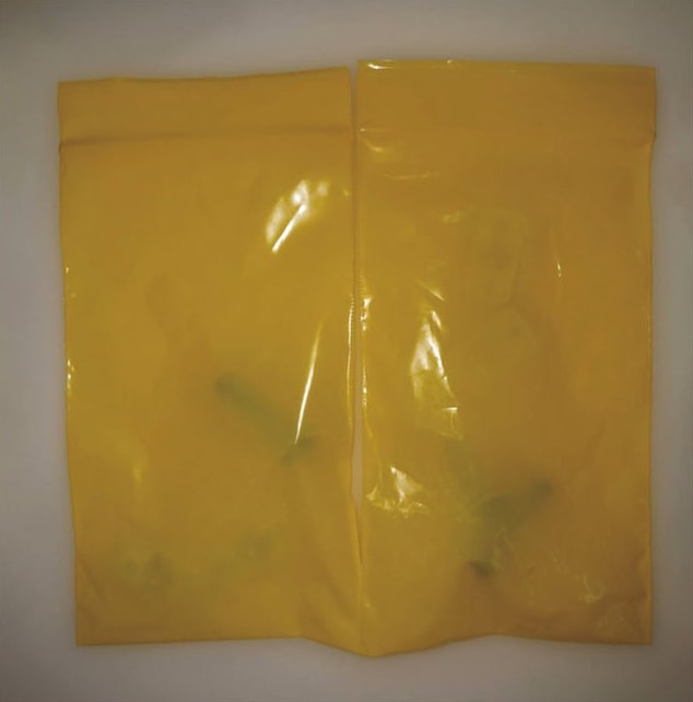
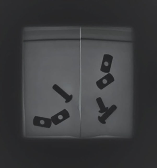
One of the most common applications for x-ray lighting is metallurgy inspection, which shows structural defects or fatigue in metal components. NIR lighting is used to present higher-contrast images in applications such as food inspection, where it becomes possible to identify nonorganic or dead products that may be present among fresh ones. Other agricultural inspection applications use NIR lighting to identify rotten fruit or vegetables. NIR is also used in waste management, recycling, and in the semiconductor industry. UV, SWIR, and LWIR are still very niche for machine vision applications.
Other Technology Developments and Trends
3D Vision
As robotic vision becomes more common and machine vision extends its support to applications beyond the plant floor, the need for accurate 3D machine vision increases. Today, designers have many different ways to solve a 3D vision application: stereovision using multiple cameras to detect 3D position based on slight changes in perspective; single-camera 3D, where images are acquired from different locations and use perspective processing similar to stereovision to determine 3D position; single camera, either area or line scan, with structured light projection; and static camera with multiple unstructured illumination sources positioned around the target (known as photometric 3D). Options abound and will only continue to grow.
In response, many machine vision camera makers now offer optimized 3D cameras with factory-calibrated measurement systems that greatly simplify the integration of 3D vision. Furthermore, GeniCam 3.0 has simplified the detection and programming of standard 3D camera solutions, removing one of the last remaining challenges to increased 3D camera market adoption.
Smart Cameras and Embedded Vision
Any discussion of embedded vision needs to start with a discussion about the future of smart cameras, because smart cameras represent the first volume application for embedded vision technology. Embedded machine vision systems combine all elements of a machine vision system, including image acquisition, image processing, and communication in a form factor that prizes compact size and low power consumption.

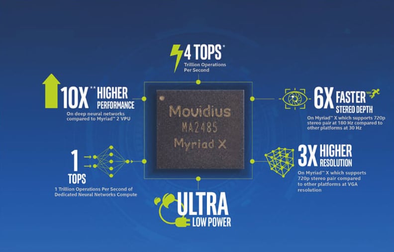
Previously, smart camera integration was done at the board level. These systems put all elements on as few boards as possible in a single enclosure. However, 2018 marked the first year that traditional machine vision companies were able to access new system-on-a-chip (SoC) solutions such as the Xilinx Xinq, which combines Arm cores and FPGA arrays on a single chip. The industry is still waiting on volume access to Intel's Movidius SoC chipset. It is safe to say that this new highly integrated vision SoC solution could significantly alter smart camera capability, performance and cost. It will open up an unprecedented market opportunity to embed machine vision in an unlimited number of nontraditional applications that would benefit from automated imaging functionality. As this report indicates, for sensor companies that sell into both the machine vision industry and nontraditional markets, the opportunities outside machine vision far exceed traditional industrial applications.
Backlight Illumination and High Dynamic Range
The ability to back-thin and therefore increase the photoactive area of the sensor to make it more sensitive, is a driving force behind the continuance of CCD sensors. At the same time, high-dynamic-range (HDR) capabilities on CMOS sensors are allowing a sensor to capture a car's license plate in near dark without being blinded by headlights just outside the camera's field of view.
Both approaches to improving the sensitivity of sensors are expected to continue, eventually leading to backlit CMOS sensors that offer more of the benefits of CCD sensors without sacrificing speed and cost.
What the Future Looks Like
As this article shows, machine vision camera technology is accelerating in adoption and diversity, making it possible for amateurs to solve simple vision sensor applications while integrators break new ground in vision-guided robotics, autonomous navigation, and other complex applications. These trends are expected to continue into the foreseeable future as the world finds new ways to empower machines — and people — by helping them see through machine vision lenses.
This article was written by Alex Shikany, Vice President of Membership & Business Intelligence with the Association for Advancing Automation (A3) and Winn Hardin, Contributing Editor for A3. For more information, contact Mr. Shikany at

