Circuit designs exploiting the increased energy storage provided by supercapacitors require more careful consideration of the increased power handling than that of batteries when charging these devices. The unique composition of electrochemical double-layer capacitors (EDLC) inherently allows them to withstand large currents. Table 1 is a brief list of AVX cylindrical (SCC) and series-connected module (SCM) SuperCapacitors, displaying peak current supply and sink current capability. These maximum specifications will typically exceed current capability of charge sources and lead to failures within the power supply system.
Supercapacitors have low equivalent series resistance (ESR), causing an uncharged supercapacitor to appear as a dead short. This will instantaneously draw maximum current from the source in an attempt to charge up to its rated capacitance [I = C x (dV/dt)]. Typically, this charge current greatly eclipses what the power source is able to supply. In many instances, the amount of current draw is so much more than what the power supply can handle that it will drive the power source or system into permanent failure or at least a transient upset.
To demonstrate this, compare the current draw by a supercapacitor to a transient containing hundreds or thousands of amps, causing significant voltage drop across sensitive circuits and resulting in bit error on high-speed transceivers, system shutdown, or software reset. In an effort to mitigate this problem, many charge limiting circuits exist but a high-level comparison of passive and active control methods can help determine which topology to implement.

Passive Charge Control Method: Fixed Resistor Versus Thermistor
Resistor
One option for a passive current limiter is to add a fixed resistor in series to the supercapacitor. The added resistance will lower the inrush current to a desired value. Even though this solution is easy to design, it is important to know that a fixed resistor will degrade the power supply and cause power loss. The power equation below demonstrates how a resistor can affect the power in a system. Another important design consideration is the efficiency of a fixed resistor solution. Since there is a significant amount of power loss, a fixed resistor will be less efficient than other current limiters.
P = I2R
Where: P=Power, I=Current,
and R=Resistance
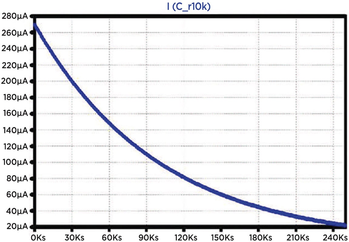
Figures 1, 2, and 3 are Spice simulations to show how fixed resistors limit inrush current. When a 10F supercapacitor is connected to a 2.7-V source, there is an immediate 27-A inrush current (Figure 1). Adding a series 150-Ω resistor, the inrush current drops to 18 mA (Figure 2). Adding a 10-KΩ drops the inrush current to 280 μA (Figure 3). To find the desired resistance, a simple Ohm’s law equation is used where I is the peak inrush current.


Thermistor

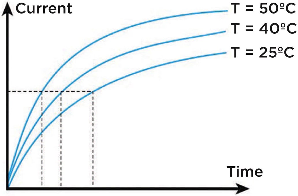
Another option for a passive current limiter is to replace the fixed resistor solution with a series Negative Temperature Coefficient (NTC) resistor, also known as a thermistor. An NTC is similar to a fixed resistor while at 25 °C. The difference is that an NTC varies resistance in accordance with a nonlinear curve that is temperature-dependent (Figure 4). At 25 °C, the thermistor starts with a defined high-resistance state, absorbing power and restricting inrush current. As the system runs, the load draws current and the NTC will heat up. When the NTC is heated, the resistance value will drop in accordance with its performance curves. With a lesser resistance, more current will flow into the supercapacitor. The effect of an NTC body temperature relayed to the current flowing into the load is shown in Figure 5.

The top section of Figure 6 is a Spice simulation that shows how the NTC (R150@25 °C) resistance decreases over time. The bottom portion of Figure 6 is a Spice simulation to show how the NTC controls the inrush current. As stated earlier, when a 10F capacitor is connected to 2.7 V, the inrush current is 27 A. When a NTC R150@25 °C is added in series, there is an inrush current of 18 mA. Comparing Figure 6 with a 150-Ω fixed resistor shown in Figure 3, it is clear that the inrush current is limited to a similar value.

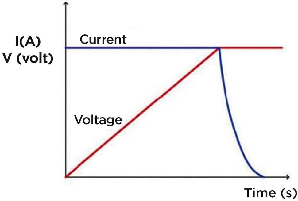
As the system runs, the NTC loses resistance and allows the current to reach a peak of 24 mA. Figure 7 shows the overall effect of an NTC upon current inrush. As the graph shows, an unprotected system will have a large current and power inrush that drops the magnitude in accordance with the capacitor charge equation shown previously. With an NTC, the thermistor will absorb power as a function of time (t=0), giving the system a manageable state.

When designing a system with an NTC, there are a few considerations to take into account. The first is the power rating and surge. The NTC’s power rating must be greater than the surge or the system will fail. The second is the thermal mass of the NTC and response time. The size of the NTC will affect how long it takes to charge the capacitor. If a large NTC is needed, the response time will increase.
Even though the NTC is more efficient than a fixed resistor and it has a lesser power loss, there are some disadvantages. For example, since the NTC depends on temperature, it can be difficult to design an NTC into an application with multiple temperatures in addition to 25 °C. Another drawback of an NTC is its cool-off time. After an NTC has heated up, it needs to be removed from the source in order to return to room temperature and high resistance. If it is not restored back to room temperature, it will not work to limit the current. Its resistance value will already be low, which will allow for high currents to flow into the capacitor. For this reason, NTCs are not recommended for use in applications with a high cycling rate.
Active Charge Control Method: MOSFET Versus Integrated Circuit
MOSFET
The simplest active charge control makes use of MOSFETs. MOSFETs work very efficiently at low voltages and have virtually no current draw; thus, they are low-power devices. However, precautions must be taken to protect these devices from transient voltages during manufacturing, assembly, and operation. Additionally, MOSFETs are susceptible to steady state overvoltage exposure.

MOSFETs work very efficiently when designed with proper caution. Figure 8 shows the fundamental implementation of a p-channel MOSFET using a low-voltage gate driver controller. The charge circuit is broken up into two sections: a load switch (Q2; p-channel MOSFET) and a gate control (Q1; n-channel MOSFET). The control FET can utilize low-voltage control signals to effect slew rate of the load switch. This circuit is based upon the fact that a small ‘control’ signal to the gate of the load switch MOSFET (Q2) can easily and accurately control the current delivered to a large supercapacitor. The disadvantage of this configuration is the need for an added MOSFET and passive components. Added components increase cost, size, and weight to the circuit but in many cases, any perceived disadvantages are outweighed by control accuracy and improved system reliability.

Integrated Circuit
IC chipsets used in conjunction with supercapacitors generally offer features grouped into:
Cell Balance Control
Current Control
Balance Control & Overvoltage Protection
Backup & Voltage Regulation
Charge control chipsets use elaborate and comprehensive active charge control methods to perform Constant Current and Constant Voltage (CC/CV) charging, with programmable input current limits (Figure 9). Many controller ICs come with built-in voltage regulation, monitoring, and multi-cell balancing when implementing a stack of supercapacitors. When implementing a stack or bank of supercapacitors, it is critical to have a balancing circuit on the supercapacitor stack that is purchased or an IC that provides active balancing.

Supercapacitor reliability and life are highly dependent on operating voltage — derating the voltage by 0.1 V of a 2.7-V rated part can extend the life of a component by a factor of 2. Making use of a CC/CV charging IC with stack voltage regulation and monitoring removes much of the heavy lifting and board space for an equivalent discrete solution but comes at a premium and sometimes limits the number of supercapacitors that can be balanced and monitored.
Conclusion
A high-level comparison of passive and active supercapacitor charging control methods emphasizes the need for a close inspection on power source and supercapacitor demands. The emphasis to consider supercapacitor demands continues to grow as capacitance values increase and supercapacitor ESRs drop.

Uncontrolled charging of an uncharged supercapacitor can result in the power supply experiencing near short conditions. The resulting dV/dt across charge supply semiconductors can either create permanent damage or a transient upset due to the voltage droop on critical power lines of the system. Multiple combinations of efficient and complex charge control schemes exist that work across the spectrum of cost, size/weight, and performance-sensitive circuits.
This article was written by Ron Demcko, Joe Hock, Ashley Stanziola, and Daniel West of AVX Corporation, Fountain Inn, SC. For more information, click here .


