Engineers at The University of Texas at Austin are leading an academic and industry all-star team that aims to revolutionize the production of semiconductor chips with a new 3D printing method. The new approach, which the researchers are calling Holographic Metasurface Nano-Lithography (HMNL), aims for faster, more efficient and environmentally friendly production of advanced electronics.
HMNL has applications ranging from smartphones to robotics to aerospace. It can create designs that were previously impossible, such as 3D printed capacitors, which store energy in electronic devices, or electronic packages that fit into unconventional spaces. For example, it would make it possible to embed artificial intelligence in customized configurations to fit the specifications of robots or rockets.
Here is an exclusive Tech Briefs interview — edited for length and clarity — with Team Lead Michael Cullinan, Associate Professor, Cockrell School of Engineering’s Walker Department of Mechanical Engineering.
Tech Briefs: What was the biggest technical challenge you faced while developing HMNL?
Cullinan: There were a number of challenges with a project this complex, but the hardest part was bringing together an entirely new materials resin chemistry with a novel optics design and exposure approach. This project has very ambitious goals for throughput, resolution, and materials properties that are very hard to meet simultaneously. Basically, we want to make something that is the size of a penny in about one minute that has 500nm features in it, and it needs to contain both insulators and conductors simultaneously patterned at that throughput and resolution. In addition, the electrical conductors need to have properties that are as good as bulk copper and the dielectrics need to be comparable to standard low-k dielectrics used in modern semiconductor packaging applications. Any one of these challenges would be difficult for current additive manufacturing approaches but the combination of all of them is really what required bringing together such a large and diverse team.
Tech Briefs: Can you explain in simple terms how it works please?
Cullinan: The HMNL process uses sub-wavelength-patterned metasurface masks (metamasks) to create multi-colored holograms in a photocurable metal-polymer hybrid resin. This process allows entire 3D, multi-material (insulators and conductors) nanostructures to be patterned using a single light exposure. In HMNL, the hybrid resin chemistry is designed such that ultraviolet (UV) light is used to pattern the silver conductor while visible light is used to pattern the polymer dielectric, enabling both types of materials to be fabricated simultaneously. In this hybrid resin, a metal-organic decomposition (MOD) silver precursor, which has inherent UV curability arising from silver’s native sensitivity to UV light, is combined with monomers, a visible light sensitive photoinitiator, and an UV light radical photoinhibitor. Upon UV exposure the silver salts heat up, leading to decomposition of the silver complexes and formation of metallic silver. At the same time, the photoinhibitions in the resin design prevent polymerization in the UV-exposed regions but allow polymerization to occur in the regions with visible light exposure. Therefore, this resin design provides selective formation of silver metal in the high intensity UV light areas of the pattern while enabling polymer formation only where the visible light pattern exists. Thus, by overlapping visible and UV light intensity patterns by precisely aligning the 3D light intensity patterns from different metasurfaces, we are able to make 3D, multi-material conductive and dielectric structures simultaneously in a single light exposure process step. A schematic of the setup is shown below.
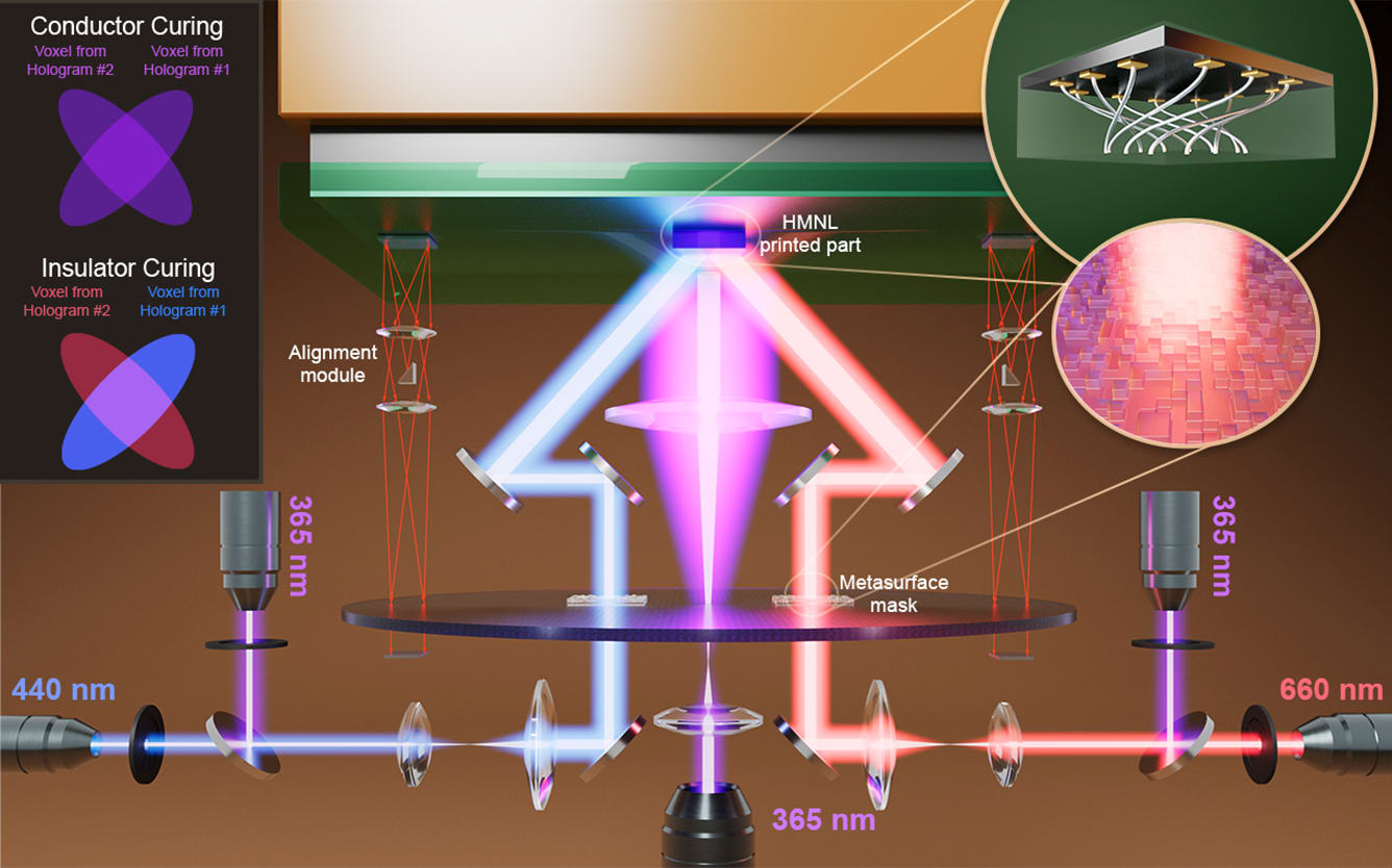
Metasurfaces are used to generate the 3D light intensity pattern in this process because metasurfaces can be encoded with much higher information density than traditional spatial light modulators such as digital micromirror devices. So, the use of metasurface optics in HMNL overcomes many of the low-resolution and small-patterning-area challenges presented by conventional holographic 3D printing approaches. Additionally, the size of the hologram produced is limited only by the size of the fabricated metasurface, which can be produced at a full wafer scale if desired. We have demonstrated the ability to fabricate structures with ~500 nm resolution over areas greater than 30 mm × 30 mm using metamasks. We have also demonstrated that metasurface optics can be designed to produce different holographic patterns when exposed to different colors of light, which can be used to create multi-material structures and to fabricate features with resolutions as small as 36 nm. Preliminary volumetric patterning using this method shows a build rate of over 20 mm3/s, which is much faster that what can be fabricated using conventional multi-step semiconductor packaging fabrication approaches.
Tech Briefs: What are your next steps? How soon could we see this technology commercialized?
Cullinan: Right now, we are working on transitioning the lab scale version of the HMNL system to a tool that could sit in a cleanroom environment inside a typical semiconductor packaging fab. To do this, we need to reconfigure the optical layout to be compatible with printing directly on wafers and add alignment optics to align the printed features to fiducial alignment marks on the chip/wafer we are printing onto. The goal is to have a prototype of this commercial scale HMNL system operating in the R&D fab at the Texas Institute for Electronics by the end of 2026 in order to start collecting the real yield and reliability data on the process that is necessary for lab-to-fab commercial transition. We a very fortunate to have a strong relationship with the Texas Institute of Electronics and both the DARPA NGMM and AMME programs to enable this type of partnership.
Tech Briefs: Is there anything else you’d like to add that I didn’t touch upon?
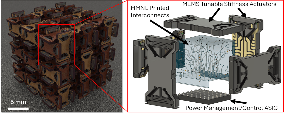
Cullinan: I think what is really exciting about this technology is not just the ability to replace how semiconductor packages are fabricated now with a faster and cheaper approach but to really rethink semiconductor packaging in general by enabling the move to true 3D package architectures. By printing non-planer interconnects, we can move beyond just stacking chips to creating 3D chiplet architectures where we have sensor arrays pointing in different directions simultaneously but working together in a single package. With this type of printing system, we could even create package architectures where the package itself is an active structure in the system, enabling completely new paradigms in the fields of robotics and metamaterials. For example, below is a robotic metamaterial structure we constructed that combines actuators and sensors in an assembly of MEMS devices to create a shape-morphing structure that is enabled by the ability to 3D print non-planar interconnect structures.