
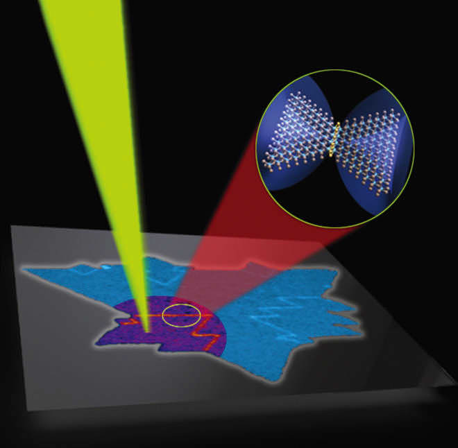
To further shrink electronic devices and to lower energy consumption, the semiconductor industry is interested in using 2D materials but manufacturers need a quick and accurate method for detecting defects in these materials to determine if the material is suitable for device manufacture. Researchers have developed a technique to quickly and sensitively characterize defects in 2D materials.
Two-dimensional materials are atomically thin — the most well-known being graphene, a single-atom-thick layer of carbon atoms. The new method uses laser light combined with second harmonic generation, a phenomenon in which the frequency of the light shone on the material reflects at double the original frequency. Dark field imaging, a technique in which extraneous light is filtered out so that defects shine through, is added, providing three times the brightness of the standard bright field imaging method and detecting types of defects previously invisible.
Dark field imaging removes the interference effects and reveal the grain boundaries and edges of semiconducting 2D materials. The technique has good spatial resolution and can image large-area samples that could be used to monitor the quality of the material produced in industrial scales.
Usually, powerful, expensive, and slow experimental probes that do microscopy using beams of electrons are needed to discern such fine details in a material. Using a fast and accessible optical method pulls out just the signal that originates from the defect itself to rapidly and reliably find out how 2D materials are stitched together out of grains oriented in different ways.
The semiconductor industry wants the ability to check for defects on the production line but 2D materials will likely be used in sensors before they are used in electronics. The next step would be an improvement of the experimental setup to map zero dimension defects — atomic vacancies, for instance — and also extend it to other 2D materials that host different electronic and structural properties.
For more information, contact Walt Mills at
More From SAE Media Group

Electronics & Sensors INSIDER
Method Detects Defects in 2D Materials for Future Electronics and Sensors

Tech Briefs
Material Increases Efficiency of LED Devices


Photonics & Imaging Technology
Essential Principles for Designing and Specifying Laser Optics

Tech Briefs
Multiplexed Optical Antennas
Photonics & Imaging Technology
New Blue Light Technique Could Enable Advances in Understanding Nanoscale Technologies
Photonics & Imaging Technology
Metasurfaces Control Polarized Light at Will
Photonics & Imaging Technology
Additive Manufacturing of Precision Optics at Micro and Nanoscale
Medical Design Briefs
New Method Detects Defects in 2D Materials
Photonics & Imaging Technology INSIDER
Light from Exotic Crystal Semiconductor Could Lead to Better Solar Cells
Medical Design Briefs
‘Seeing’ Nonuniformities in 2D Materials May Lead to New Medical Sensors
Tech Briefs
Wavy Surfaces for Better Light Control
Photonics & Imaging Technology INSIDER
Laser Pulse Creates Frequency Doubling in Amorphous Dielectric Material
Photonics & Imaging Technology INSIDER
Infrared Imaging by Ultrathin Nanocrystal Layers
