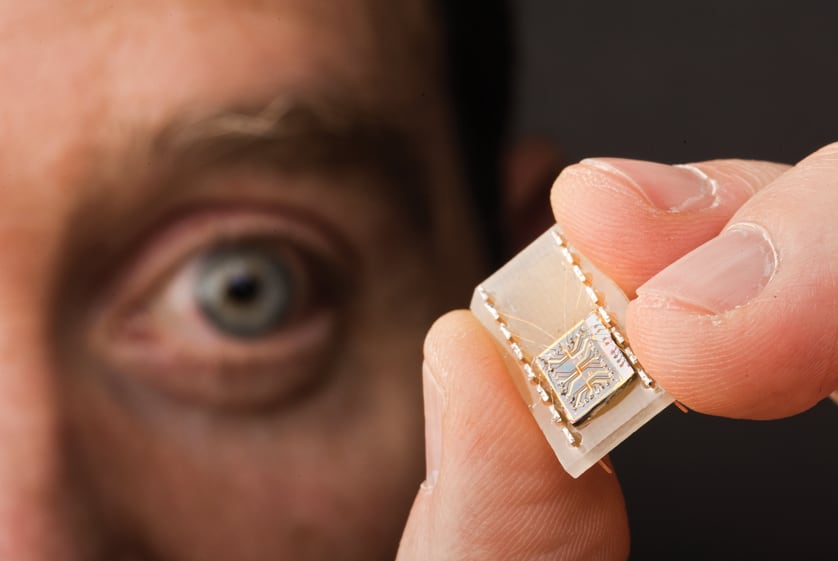
“People have been working on nanowires for 20 years,” says lead researcher Mike Lilly. “At first, you study such wires individually or all together, but eventually you want a systematic way of studying the integration of nanowires into nanocircuitry. That’s what’s happening now. It’s important to know how nanowires interact with each other rather than with regular wires.”
For years, the best available test method required researchers to put a charged piece of material called a gate between two nanowires on a single shelf. The gate, flooded with electrons, acted as a barrier - it maintained the integrity, in effect, of the wires on either side of it by repelling any electrons attempting to escape across it. But the smallest wire separation allowed by the gate was 80 nanometers. Nanowires in future devices will be packed together much more closely, so a much smaller gap was necessary for testing.
The current test design is very simple. What Lilly and colleagues at McGill University in Montreal envisioned was to put the nanowires one above the other, rather than side by side, by separating them with a few atomic layers of extremely pure, home-grown crystal. This allowed them to test nanowires separated vertically by only 15 nanometers — about the distance next-generation devices are expected to require. And because each wire sits on its own independent platform, each can be independently fed and controlled by electrical inputs varied by the researchers.
(Sandia National Laboratories)

