
As thin-film technology advances, it’s increasingly important to monitor the film’s characteristics. That’s because eliminating irregularities in thin films — used primarily to create computer chips — enhances their performance. k-Space Associates (kSA, Ann Arbor, MI) specializes in accurate, precise monitoring methods that allow physicists and engineers to create high-performance thin-film products and improve their research and development workflow.
Assessing Film Quality
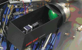
The camera is always outside of the deposition chamber. When the film is probed with the electron beam, it is diffracted off the surface of the film, and the diffracted beam then hits a phosphor screen, which is inspected through a glass viewport and analyzed by acquiring real-time images of the screen with the camera. If the film is probed with laser beams, then the directly reflected beams come through the glass viewport and directly hit the CCD sensor chip. The beam positions and profiles are then analyzed.
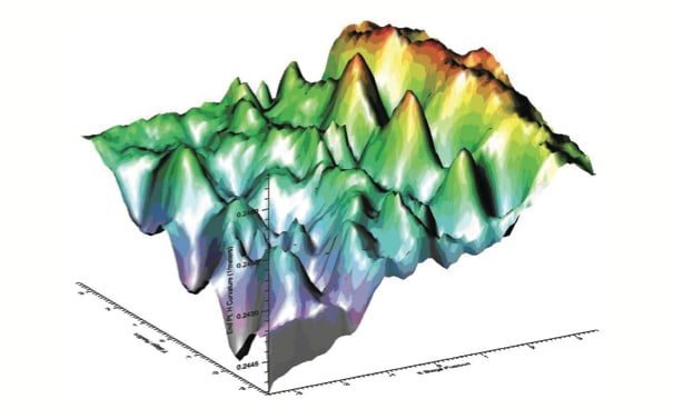
Analyzing and intuitively representing these reflected beams allows scientists to improve the quality and performance of the thin-film devices, which range from memory storage, to computer processors, to light-emitting diodes (LEDs). kSA processes the patterns, oscillations, and intensity variations using mathematical routines in IDL data visualization and analysis software from ITT Visual In- formation Solutions (Boulder, CO), giving users the data and visualizations they need in a graphical user interface.
Darryl Barlett, general manager and founder of kSA, chose IDL to integrate with his product line for a number of reasons. “There is a plethora of advanced mathematical analysis routines in IDL that we make use of in analyzing the processed data. We use IDL for all our display capabilities because IDL does such a good job with graphical representation.”
IDL math routines used in the analysis include a curve-fitting procedure general-function fitting routine to fit a damped sine wave to intensity data acquired in real time. The IDL cubic spline and polynomial fitting routines are used to generate data calibration files with a functional dependence (instead of needing the raw data).
After originally using a third-party graphics package for data display, Barlett and his team incorporated IDL as their products increased in complexity and functionality. Other tools could not manage and represent the data efficiently and effectively, and they lacked important mathematical capabilities.
As specialists in in-situ monitoring, kSA recognizes that semiconductor devices will continue to get smaller, more powerful, faster, and that the monitoring process will become even more critical to effective production. They plan to continue developing their product lines to keep pace with technology and to keep IDL an integral part of their offering.