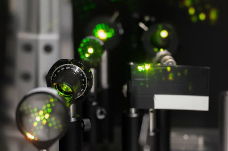
Physical chemists at the Georgia Institute of Technology discovered an emerging class of semiconductors with some unexpected moves. Despite a wobbling molecular motion, the hybrid-organic-inorganic perovskites, or HOIPs, open up the possibility of new applications in areas from lasers to LEDs.
In an international study , the team successfully measured a prototypical HOIP and found that its quantum properties are on par with established, molecularly rigid conductors like silicon, graphene, and gallium arsenide.
“At room temperature, the molecules wiggle all over the place,” said Carlos Silva, a co-author of the study and a professor in Georgia Tech’s School of Chemistry and Biochemistry. “But surprisingly, the quantum properties are really stable.”
The hybrid includes inorganic layers of the rigid lead iodide, separated by the rubber-like organic layers of phenylethylammonium.
The HOIPs operate at room temperature without requiring ultra-cooling – a characteristic that sets the perovskites up for practical use as semiconductors. With an additional ability to absorb and emit light well, the material may also support new applications related to lasers, LEDs, and photovoltaics.
Researchers like Carlos Silva and physicist Ajam Ram Srimath Kandada are still figuring out how stable quantum properties are achieved through such unsteady molecular activity.
Silva, co-author of the study, spoke with Tech Briefs about why the hybrid-organic-inorganic perovskites have such exciting potential.
Tech Briefs: What inspired this work?
Silva: We are fascinated by interactions between particles in solids, especially semiconductors, because these interactions have important consequences on how the particles behave in optoelectronic devices. We are particularly interested in understanding how multiple charges “dance together” in the material when they are in a structure that is fluctuating and shaking.
Tech Briefs: What exactly are hybrid organic-inorganic perovskites (HOIPs)?
Silva: “Perovskite” refers to the crystal structure of the material. It tells us how the atoms are arranged in space in a regular, periodic fashion. “Hybrid” refers to the fact that these crystals are composed of a periodic array of both organic (carbon-based floppy molecules) and inorganic (the more rigid lead and iodine) constituents.
Tech Briefs: How do HOIPs differ from established semiconductors?
Silva: The material is unlike established semiconductors like gallium arsenide, which is assembled in three dimensions in a rigid array of gallium and arsenic atoms. The rigidity of the traditional semiconductors is important in defining their good electronic properties, such as electrical transport. Hybrid semiconductors, however, allow fine control of their structure, and therefore the electronic properties, because of the ability to make different organic components with tailored structural properties.
Tech Briefs: What kinds of tailored structural properties are possible?
Silva: For example, we made and studied two-dimensional perovskites that are 2D because of the organic molecules that we chose to use. If we choose different ones, they may be 3D or anything in between.

Tech Briefs: How does the use of organic molecules impact the behavior of the HOIPs?
Silva: One important consequence of the use of organic molecules is that these shake and wiggle quite a bit, particularly at ambient conditions, and one important question relates to how the molecular motion induces “noise” — uncorrelated motion — in the organic lattice.
Tech Briefs: How does this noise affect the semiconductor properties of these materials?
Silva: We know from extensive work in this community that the devices function well, and that charge transport is good. However, we wanted to understand how excited-state particles in 2D perovskites, so-called excitons and bi-excitons, respond to the noise in the structure. We were surprised to find that bi-excitons are as stable as in other more rigid, emerging materials like transition-metal dichalchogenides (such as molybdenum disulphide), although hybrid perovskites are micro structurally more complex (but simpler to manufacture). This tells us something about how important interactions between electrons are in perovskites.
Tech Briefs: What is special about the semiconducting properties of HOIPs?
Silva: The excitement in our community over the last few years has stemmed from the fact that in spite of the complexity of the hybrid perovskite crystal lattices, both in terms of its structure and its noisy fluctuations, their semiconductor properties are actually very good and compete quite nicely with established semiconductors.
Solar cells are now made with this class of materials with power conversion efficiencies that rival established technologies, but by solution processing. Other optoelectronic technologies such as LEDs and lasers are not far behind. The challenge with these materials are in terms of their stability and environmental considerations, but our friends, the synthetic-materials chemists and engineers, are working on these issues.
Tech Briefs: Why is solution processing important?
Silva: Because these semiconductors are made by solution, we can make different semiconductor structures simply and with low-energy consumption. In contrast, 2D gallium arsenide structures need to be fabricated with very precise epitaxial control, which involves high temperature processing, and highly sophisticated semiconductor engineering. Playing with the structure of these is much harder.
Tech Briefs: What is possible with these kinds of inorganic and organic properties?
Silva: This is exciting for the understanding of the materials at a fundamental level, but it also enables technologies that are based on light emission. For example, if we are able to make these hybrid excitations, with the desired properties of both organic and inorganic semiconductors simultaneously, we might be able to make coherent light emitters akin to lasers, but with much lower threshold, and with lower-energy processing.
Tech Briefs: What’s next? What will you be working on as it relates to HOIPs?
Silva: We will be extending our work to study 2D perovskites with very systematically controlled crystal structure via modification of the organic component, and ask how the noisy lattice motion that we highlighted in our recent paper changes, and therefore how the light-induced excitations respond. We will put these materials in optical cavities to study the light-matter coupling in different regimes, and follow the consequences of structure/property relationships all the way to device function.
We have a broad playground for the optical semiconductor physics of these exciting materials, and we will play! It is exciting that this understanding may truly lead to new technologies.
What do you think? Share your thoughts below.

