
Small electric power cells based on the direct conversion of kinetic energy of alpha particles into electricity have been proposed. These cells are expected to function continuously over long times and at temperatures from -250 to 600 °C. They would be made from semiconductors that are stable at high temperatures (most likely GaAs or SiC). The a-particle sources in these cells will likely be made from curium-244, the radioactivity of which is characterized by a half-life of about 18 years and consists nearly entirely of a particles. The proposed cells could be useful as power sources for low-power electronic circuits that are required to operate for long times without recharging or external wire power connections, and without relying on sunlight. Potential outer-space and terrestrial applications could include electronic circuits for spacecraft on long interplanetary or deep-space missions, hearing aids, and surgically implanted medical electronic devices.
Earlier attempts at utilizing a particles to generate electricity have resulted in limited success because of poor planning and lack of proper device designs. Therefore, the planned development of the proposed cells will include studies of factors that affect power-generation efficiency and of the ability of the cells to survive lattice damage induced by impinging a particles. Computer simulations of the effects of different levels of doping of the semiconductors will be performed in an effort to find optimum device designs, and innovative and device engineering is planned to minimize lattice damage from a particles to maximize device lifetimes and reliabilities.
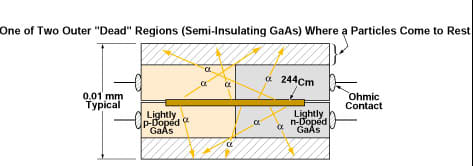
A basic power cell according to the proposal would include a thin-film a-particle source sandwiched between two p/n diodes (see figure). One key aspect of design that would clearly distinguish a cell of this type from, say, a photovoltaic cell would be the choice of diode dimensions so that a particles of the given initial kinetic energy ( ≈ 5.9 MeV for a 244Cm source) do not stop in the active device volume. The reason for this choice is that a particles cause severe lattice damage in the vicinities of their stopping locations because they lose large fractions of their kinetic energy just before stopping.
Therefore, in the proposed design, outer regions of "dead" semiconductor material would be provided and the dimensions of the p, n, and outer regions would be chosen so that the a particles would come to rest in the outer regions. Although some lattice damage is still expected to occur in the active regions, it has been observed in recent experiments that such damage is continuously annealed during ionization processes in semiconductors.
This work was done by Jagdishbhai Patel of Caltech for NASA's Jet Propulsion Laboratory. For further information, access the Technical Support Package (TSP) free on-line at www.techbriefs.com under the Electronic Components and Systems category.
NPO-20654
This Brief includes a Technical Support Package (TSP).
Generating Electric Power from Alpha-Particle Sources
(reference NPO20654) is currently available for download from the TSP library.
Don't have an account?
Overview
The document outlines a novel technology for generating electric power from alpha-particle sources, developed by Jagdishbhai U Pate1 at NASA's Jet Propulsion Laboratory (JPL). This technology addresses the critical need for reliable and long-lasting power sources for space exploration and miniaturized consumer electronics, particularly in extreme temperature conditions.
The key innovation lies in the design of a semiconductor p-n junction device that efficiently converts the kinetic energy of alpha particles, specifically those with energies between 5.8 to 6.1 MeV, into electricity. The design ensures that these alpha particles do not stop within the active device volume, as their stopping would cause significant lattice damage. Instead, the technology protects the active volume from such damage, enhancing the durability and functionality of the device.
The motivation for this development stems from the limitations of conventional power sources, which become inefficient at very low temperatures (below -15°C) encountered during deep space missions, and at high temperatures (above 350°C) where inter-diffusion of materials can destroy electronic devices. Additionally, traditional solar power generation is heavily reliant on light intensity, which diminishes in deep space missions where sunlight is obscured.
The proposed alpha-particle power source utilizes curium-244, an isotope with a half-life of 16 years, making it suitable for long-duration applications. The technology promises to provide continuous power without the need for recharging, making it ideal for powering microelectronic circuits in a distributed power system. This could eliminate interference between circuit chips caused by traditional power distribution methods.
Furthermore, the document highlights the potential applications of this technology in medical devices, such as hearing aids, where a compact and long-lasting power source is essential. The integration of these power sources on semiconductor chips could lead to self-sufficient devices that operate effectively under extreme conditions.
In summary, this innovative approach to power generation from alpha particles represents a significant advancement in energy technology, with the potential to enhance the performance and longevity of electronic devices in both space exploration and consumer applications.