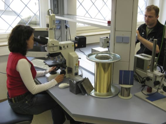
Dr. Rainer Kübler of Fraunhofer Institute for Mechanics of Materials IWM, explains, “When slicing the wafers, the challenge is to reduce the saw gap width.” The space between two wafers is governed by the thickness of the wire. The steel wire is wetted with a type of paste (slurry), a mixture of silicon carbide and polyethylene glycol. This is harder than silicon and cuts through the ingot. The gap arises where the silicon is reduced to powder during cutting. “Gap widths are currently around 180 µm,” says Kübler, “which means that given a wafer thickness of 180 µm, we generate the same amount of waste for each silicon slice. That’s inefficient.”
The researchers want to achieve smaller saw gap widths of around 100 µm, which are also suitable for industrial applications. In a project funded by the federal ministry for the environment, they are currently studying the abrasion process and contact regimes using a single-wire saw, and are principally interested in the interactions between the wire, slurry, and silicon. They are also using computer modeling to simulate different configurations. The researchers are currently striving to achieve gap widths of 90 µm, which would represent a huge increase in efficiency as waste would be halved.

