
A proposed computer architecture would exploit the capabilities of commercially available field-programmable gate arrays (FPGAs) to enable computers to detect and recover from bit errors. The main purpose of the proposed architecture is to enable fault-tolerant computing in the presence of single-event upsets (SEUs). [An SEU is a spurious bit flip (also called a soft error) caused by a single impact of ionizing radiation.] The architecture would also enable recovery from some soft errors caused by electrical transients and, to some extent, from intermittent and permanent (hard) errors caused by aging of electronic components.
A typical FPGA of the current generation contains one or more complete processor cores, memories, and high speed serial input/output (I/O) channels, making it possible to shrink a board-level processor node to a single integrated-circuit chip. Custom, highly efficient microcontrollers, general-purpose computers, custom I/O processors, and signal processors can be rapidly and efficiently implemented by use of FPGAs. Unfortunately, FPGAs are susceptible to SEUs. Prior efforts to mitigate the effects of SEUs have yielded solutions that degrade performance of the system and require support from external hardware and software.
In comparison with other fault-tolerant-computing architectures (e.g., triple modular redundancy), the proposed architecture could be implemented with less circuitry and lower power demand. Moreover, the fault-tolerant computing functions would require only minimal support from circuitry outside the central processing units (CPUs) of computers, would not require any software support, and would be largely transparent to software and to other computer hardware.
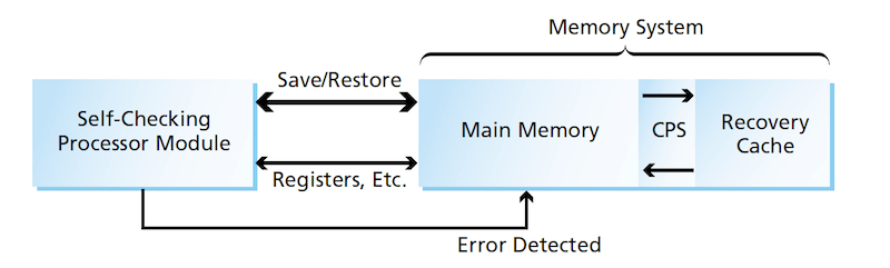
There would be two types of modules: a self-checking processor module and a memory system (see figure). The self checking processor module would be implemented on a single FPGA and would be capable of detecting its own internal errors. It would contain two CPUs executing identical programs in lock step, with comparison of their outputs to detect errors. It would also contain various cache local memory circuits, communication circuits, and configurable special-purpose processors that would use self-checking checkers. (The basic principle of the self-checking checker method is to utilize logic circuitry that generates error signals whenever there is an error in either the checker or the circuit being checked.)
The memory system would comprise a main memory and a hardware-controlled check-pointing system (CPS) based on a buffer memory denoted the recovery cache. The main memory would contain random-access memory (RAM) chips and FPGAs that would, in addition to everything else, implement double-error-detecting and single-error correcting memory functions to enable recovery from single-bit errors.
The main purpose served by the memory system as a whole would be to enable the computer to return to a valid state — a known good point reached in the computations before the occurrence of a detected error. In operation, the checkers in the self-checking processor module would signal errors to the memory system. Recovery would involve halting the operation of the self-checking processor module, correcting its configuration bits if necessary, reloading its registers, and returning control to a previous, known good point in the program. The CPUs could then resume correct computations.
The known good point in the computations would be provided by the CPS in a procedure denoted, variously, as checkpointing and checkpoint recovery or checkpoint rollback. The CPS would periodically command each CPU to store the contents of its registers in the recovery cache and clear its caches. This action would establish a checkpoint. Then the original value and the address of any clean RAM block that was subsequently overwritten by the CPU would be stored in a special RAM within the recovery cache. Subsequent writes to that block would be carried out normally (that is, without intervention by the recovery cache). If an error in the CPU were detected, the data in the special recovery-cache RAM could be used to restore the corresponding data in the main memory to their prior correct values, the processor configuration would be reloaded, the caches in the processor module would be cleared, and the processor registers restored to their prior values.
A new checkpoint could be ordered when the recovery cache became filled to capacity. Alternately, checkpoints could be forced at strategic points in the software. Another alternative would be to force checkpoints periodically, at intervals short enough to ensure that rollback time did not exceed a value that could be specified by design.
This work was done by Raphael Some and David Rennels of Caltech for NASA's Jet Propulsion Laboratory. NPO-30806.
This Brief includes a Technical Support Package (TSP).
FPGA-Based, Self-Checking, Fault-Tolerant Computers
(reference NPO-30806) is currently available for download from the TSP library.
Don't have an account?
Overview
The document is a Technical Support Package from NASA, detailing advancements in FPGA-based, self-checking, fault-tolerant computers, particularly for aerospace applications. It emphasizes the need for reliable computing systems in space, where radiation-induced errors can significantly impact performance. The technology described focuses on automatic recovery mechanisms that mitigate the effects of single event upset (SEU) errors, which are common in space environments.
Key features of the system include a hardware-mediated checkpoint recovery process. The Memory System (MS) maintains a "Recovery Cache" that allows the processor to store its register contents and clear its caches upon initiating a checkpoint. If an error occurs, the recovery cache restores the main memory to its original state, reloading the processor configuration and clearing its caches. This process is designed to minimize system impact and can be triggered automatically or by external processors.
The document also discusses the architecture of the computing elements, which utilize dual PPC 405 processors in the Virtex Pro II chip, with future versions expected to support more processors. These processors operate in lock-step, executing identical programs to enhance error detection capabilities. The design allows for high throughput and low power consumption, making it suitable for various spacecraft applications.
Moreover, the technology leverages state-of-the-art commercial off-the-shelf (COTS) hardware, providing significantly higher performance compared to traditional radiation-hardened computers while maintaining lower power, mass, and volume requirements. This flexibility allows for easy customization of computing elements for different instruments or subsystems, accommodating various digital I/O and spacecraft interface buses.
Despite the robust error recovery mechanisms, the document acknowledges the potential for multiple errors due to extreme conditions, such as solar events. Therefore, it is recommended that a lower-performance, hardened spacecraft control processor be available to manage situations where the high-performance processor cannot recover independently.
In conclusion, the document highlights the significant advancements in FPGA technology for space applications, emphasizing automatic error detection and recovery, high performance, and flexibility, which collectively enhance the reliability of computing systems in challenging environments.