
Internet of Things (IoT) applications — whether for city infrastructures, factories, or wearable devices — use large arrays of sensors collecting data for transmission over the Internet to a central, cloud-based computing resource. Analytics software running on the cloud computers reduces the huge volumes of generated data into actionable information for users, and commands to actuators back out in the field.

Sensors are one key factor in IoT success, but these are not conventional types that simply convert physical variables into electrical signals. They have needed to evolve into something more sophisticated to perform a technically and economically viable role within the IoT environment.
This article reviews the IoT’s expectations of its sensors — what must be done to achieve the large sensor array’s characteristic of the IoT. Then it addresses how manufacturers have responded with improvements to fabrication, more integration, and built-in intelligence, culminating in the concept of the smart sensors now in wide use.
It will become evident that sensor intelligence, apart from facilitating IoT connectivity, also creates many more benefits related to predictive maintenance, more flexible manufacturing, and improved productivity.
What Does the IoT Expect of its Sensors?
Sensors have traditionally been functionally simple devices that convert physical variables into electrical signals or changes in electrical properties. While this functionality is an essential starting point, sensors need to add the following properties to perform as IoT components:
Low cost, so they can be economically deployed in large numbers
Physically small, to “disappear” unobtrusively into any environment
Wireless, as a wired connection is typically not possible
Self-identification and self-validation
Very low power, so it can survive for years without a battery change, or manage with energy harvesting
Robust, to minimize or eliminate maintenance
Self-diagnostic and self-healing
Self-calibrating, or accepts calibration commands via wireless link
Data pre-processing, to reduce load on gateways, PLCs, and cloud resources
Information from multiple sensors can be combined and correlated to infer conclusions about latent problems; for example, temperature sensor and vibration sensor data can be used to detect the onset of mechanical failure. In some cases, the two sensor functions are available in one device; in others, the functions are combined in software to create a ‘soft’ sensor.
The Manufacturers’ Response: Smart Sensor Solutions
This section looks at the smart sensors that have been developed for IoT applications in terms of both their building blocks and their fabrication, and then reviews some of the advantages that accrue from the sensors’ in-built intelligence, especially the possibilities for self-diagnostics and repair.
What’s in a Smart Sensor and What is it Capable of?
We’ve reviewed the IoT’s expectations of a smart sensor, but how has the industry responded? What’s built into a modern smart sensor, and what is it capable of?
Smart sensors are built as IoT components that convert the real-world variable that they’re measuring into a digital data stream for transmission to a gateway. Figure 1 shows how they do this. The application algorithms are performed by a built-in microprocessor unit (MPU). These can run filtering, compensation, and any other process-specific signal conditioning tasks.
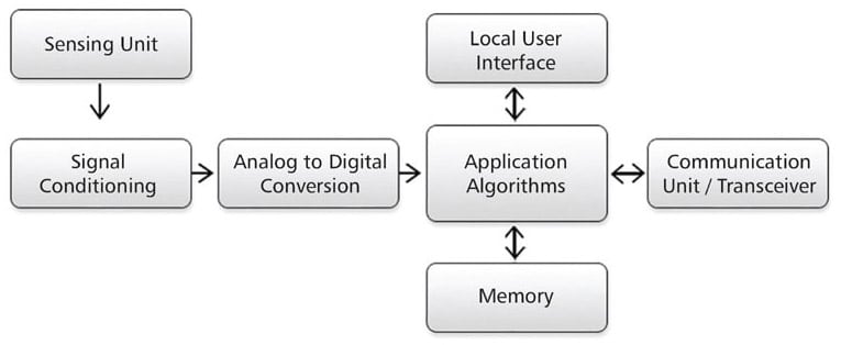
The MPU’s intelligence can be used for many other functions as well to reduce the load on the IoT’s more central resources; for example, calibration data can be sent to the MPU so the sensor is automatically set up for any production changes. The MPU can also spot any production parameters that start to drift beyond acceptable norms and generate warnings accordingly; operators can then take preventative action before a catastrophic failure occurs.
If appropriate, the sensor could work in “report by exception” mode, where it only transmits data if the measured variable value changes significantly from previous sample values. This reduces both the load on the central computing resource and the smart sensor’s power requirements — usually a critical benefit, as the sensor must rely on a battery or energy harvesting in the absence of connected power.
If the smart sensor includes two elements in the probe, sensor self-diagnostics can be built in. Any developing drift in one of the sensor element outputs can be detected immediately. Additionally, if a sensor fails entirely — for example, due to a short-circuit — the process can continue with the second measuring element. Alternatively, a probe can contain two sensors that work together for improved monitoring feedback.
Smart Sensor: A Practical Example
An application developed by Texas Instruments provides a practical example of a smart sensor, and how its building blocks work together to generate useful information from analog current and temperature measurement, as well as providing the intelligence for the other functions mentioned. The application uses a variant of their ultra-low-power MSP430 MCU range to build a smart fault indicator for electric power distribution networks.
When properly installed, fault indicators reduce operating costs and service interruptions by providing information about a failed section of the network. At the same time, the device increases safety and reduces equipment damage by reducing the need for hazardous fault-diagnostic procedures. Fault indicators, due to their location, are primarily battery-powered, so low-power operation is also highly desirable.
The fault indicators — which are installed on the junctions of the overhead power-line network — send measurement data about the temperature and current in power transmission lines wirelessly to the concentrator/terminal units mounted on the poles. The concentrators use a GSM modem to pass the data to the cellular network to relay realtime information to the main station. The main station can also control and run diagnostics on the fault indicators through this same data path.
Continuous connection to the main station has several advantages. The first is the ability to remotely monitor fault conditions rather than searching for them in the field. A smart fault indicator can also constantly monitor temperature and current so that the controller at the main station has real-time status information about the power distribution network. Accordingly, power utility providers can quickly identify the fault location, minimize power downtime, and even take action before a failure occurs. Workers at the main station can run diagnostics on the fault indicators at required intervals to check that they are working correctly.
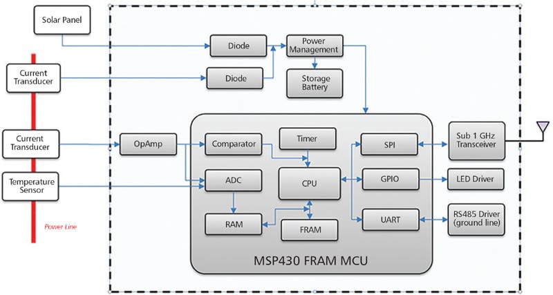
Figure 2 is a functional block diagram of such a smart fault indicator based on the TI MSP430 ferroelectric random-access memory (FRAM) microcontroller (MCU). The current transducer produces an analog voltage proportional to power-line current. An operational amplifier (op amp) amplifies and filters this voltage signal. The analog-to-digital converter (ADC) on the MCU samples the output of the op amp. The digital stream from the ADC is then analyzed by software running on the CPU or accelerator. The op amp output is also connected to a comparator on the MCU. The comparator generates a flag to the central processing unit (CPU) in the MCU if the input level transgresses a predetermined threshold.
The MSP430’s computing power allows frequency-domain current measurement analysis that provides a deeper insight into power line status than previous time-domain methods. The fast FRAM read-and-write speeds enable the accumulation of data for pattern analysis, while the MCU’s ultra-low-power operating modes allow extended battery life operation.
Fabrication
To realize the full potential of the IoT, sensor fabrication methods must continue to reduce the size, weight, power, and cost (SWaP-C) of the sensor component and system. The same trend needs to apply to sensor packaging, which currently accounts for as much as 80% of the overall cost and form factor.
Smart sensors form when micro-electromechanical system (MEMS) sensor elements are closely integrated with CMOS integrated circuits (ICs). These ICs provide device bias, signal amplification, and other signal processing functions. Originally, the wafer-level vacuum packaging (WLVP) technology used included only discrete sensor devices, and smart sensors were realized by connecting discrete MEMS chips to IC chips through the package or board substrate in an approach called multi-chip integration. An improved approach interconnects the CMOS IC and sensor elements directly, without the use of routing layers in the package or board, in a construction known as a system-on-chip (SoC). When compared to the discrete multi-chip packaging approach, SoC is typically more complex but leads to reduced parasitics, smaller footprints, higher interconnect densities, and lower package costs.
Other Advantages of Smart Sensor Intelligence
Smart photoelectric sensors can detect patterns in an object structure and any changes in them. This happens autonomously in the sensor, not in any external computing element. This increases processing throughput and reduces the central processor — or local PLC’s — processing load.
Manufacturing flexibility is improved — a vital advantage in today’s competitive environment. Intelligent sensors can be remotely programmed with suitable parameters every time a product change is required. Production, inspection, packaging, and dispatch can be set for even single-unit batch sizes at mass-production prices, so each consumer can receive a personalized, one-off product.
Feedback from linear position sensors has traditionally been hampered by problems relating to system noise, signal attenuation, and response dynamics. Each sensor needed tuning to overcome these problems. Honeywell offers a solution with their SPS-L075-HALS Smart Position Sensors. These can self-calibrate by using a patented combination of an ASIC and an array of MR (magne-toresistive) sensors. This accurately and reliably determines the position of a magnet attached to moving objects such as elevators, valves, or machinery.
The MR array measures the output of the MR sensors mounted along the magnet’s direction of travel. The output and the MR sensor sequence determine the nearest pair of sensors to the center of the magnet location. The output from this pair is then used to determine the position of the magnet between them. This non-contacting technology can provide enhanced product life and durability with less downtime. A self-diagnostics feature can further reduce downtime levels.
These sensors also tick other IoT smart sensor requirements. Their small size allows installation where space is at a premium, while IP67 and IP69K sealing options allow deployment in harsh environments. They are smart enough to replace several sensor and switch components together with the extra wiring, external components, and connections also previously needed. The sensors are used in aerospace, medical, and industrial applications.
Smart Sensors with Self-Diagnostics and Repair Capabilities
Smart sensors can also be well-suited to safety-critical applications like detection of hazardous gas, fire, or intruders. Conditions in these environments can be harsh, and the sensors can be difficult to access for maintenance or battery replacement, yet high reliability is critical. A team at the Lab-STICC Research Center, University of South-Brittany, has been developing a solution that improves reliability by using dual probes and hardware that can self-diagnose and repair itself.
The ultimate goal of their project is to integrate all the elements described into a single discrete device, suitable for applications such as hazardous gas detection in areas such as harbors or warehouses. The project centers on a node that can pinpoint an internal failure and take corrective action to improve both reliability and energy efficiency. This reduces the node’s vulnerability and alleviates maintenance costs. The design recognizes the limitations of such sensors: restricted battery autonomy, energy harvesting subject to unreliable energy source behavior, limited processing and storage resources, and a need for wireless communications.
The node is equipped with two sensors; during normal operation, the first captures environmental data while the second is only activated by users to verify the obtained data. If the first sensor were to fail, the node’s reliability is downgraded, while battery power is being wasted on supplying the non-functioning sensor. However, if the node disconnects the first sensor and switches to the second, no energy is wasted and node reliability is maintained.
Accordingly, the project’s objective was to develop a novel self-diagnostic based on functional and physical tests to detect a hardware failure in any component of the wireless sensor node. This method can identify exactly which node component has failed and indicate suitable remedial action.
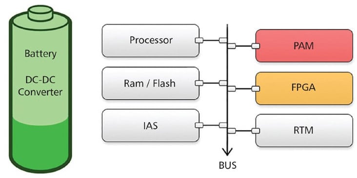
Figure 3 shows the hardware configuration of the self-reconfigurable sensor node. Its components include a processor, a RAM/FLASH memory, an Interface for Actuator and Sensors (IAS) to interface with the environment, a Radio Transceiver Module (RTM) to transmit and receive data, and a battery with power switches (DC-DC converters). The node also includes a Power and Availability Manager (PAM) combined with an FPGA-configurable zone. The first one is considered as the intelligent part for the best use of energy, auto-diagnosis, and fault-tolerance, while the other enhances the availability of the sensor node.
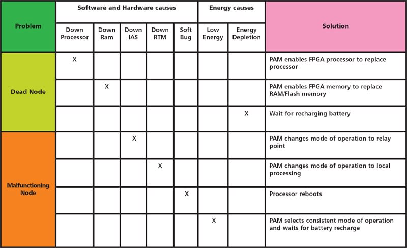
The table in Figure 4 shows how the sensor node can respond to various node issues. The FPGA contains a softcore 8051 CPU that is activated when performance enhancement is needed or to replace the main processor if it fails. The FPGA is an Actel type IGL00V2, chosen for its reliability and low power consumption. The remainder of the node comprises a PIC processor, RAM memory, Miwi radio transceiver module, two Oldham OLCT 80 gas detectors, LM3100 and MAX618 power switches, and a battery.
Conclusion
In this article, we have seen how chip manufacturers and researchers have been responding to the IoT’s need for smart sensors. This has partly been a matter of adding intelligence and communications capabilities to the basic transducer function, but it also involves improved fabrication. By integrating the MEMS sensor elements and CMOS computing components onto a single substrate, smart sensors can be implemented in small, low-cost packages that can be embedded in space-constrained applications with resilience to their environmental conditions.
Accordingly, IoT designers can source the sensors that they need — small, cheap, resilient, and low-power enough for ubiquitous deployment, while having the intelligence to deliver useful information as well as raw data. They also facilitate more flexible, granular automation, as they can accept incoming commands for recalibration to accommodate production changes.
This article was contributed by Newark element 14, Chicago, IL. For more information, Click Here .