Stories
35
66
0
690
30
Briefs: Imaging
Today's glass-based lenses are bulky and resist miniaturization. To address the problem, two different imaging methods — a type of lens designed for nanoscale interaction with lightwaves, and robust...

INSIDER: Photonics/Optics
Northern Arizona University assistant professor Ryan Behunin collaborated with a team of physicists from Yale and the University of Texas at Austin in discovering an innovative way...

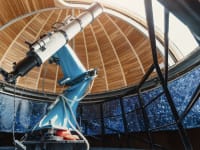
INSIDER: Imaging
A research project designed to enable more precise imaging of space objects has moved from lab bench testing to field testing at the John Bryan State Park observatory,...

INSIDER Product: Photonics/Optics
CMOS Image Sensor
Teledyne e2v (Chelmsford, UK) recently announced its Emerald 67 megapixel, the newest member of its Emerald CMOS image sensor family. The new sensor features a high resolution with a small global shutter pixel...

Products: Test & Measurement
Trilinear Line Scan Cameras
Teledyne e2v (Milpitas, CA) has announced its next generation of line scan cameras — the high-resolution ELiiXA+ trilinear color range. These new 8k pixel cameras are suited for industrial applications...

Articles: Photonics/Optics
“Measurement is the first step that leads to control and eventually to improvement. If you can’t measure something, you can’t understand it....

Articles: Materials
Today’s high-resolution laser scanning confocal microscopes (LSCM), also referred to simply as laser scanning microscopes, are powerful high-magnification surface metrology instruments with a...

Application Briefs: Semiconductors & ICs
The demand for innovative solutions to enhance the safety of military personnel is continually on the rise. This includes the need to improve the performance of military vehicles and aircraft, in terms of both safety...

Articles: Lighting
The task of creating a streetlamp optical system has changed over the last 20 years and due to this change, so has optical design software. Let’s compare the task of designing...

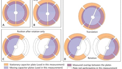
Briefs: Photonics/Optics
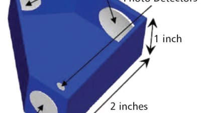
Positional sensors have applications where a very accurate measurement of position is needed over a limited range. One example of such an application is in manipulation of a stage...
Articles: Manufacturing & Prototyping
This column presents technologies that have applications in commercial areas, possibly creating the products of tomorrow. To learn more about each technology, see the contact information provided for that innovation.

Briefs: Photonics/Optics
Rice engineers have developed a wide-field microscope thinner than a credit card, small enough to sit on a fingertip and capable of micrometer resolution over a volume of several cubic millimeters.
Articles: Photonics/Optics
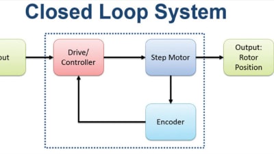
Step motors are widely used in automation due to their high resolution, precision positioning, minimal control electronics, and low cost. As an open loop system, traditional...
Articles: Photonics/Optics
In the traditional model of healthcare, a patient would visit a doctor regularly for checkups or for evaluations when there’s an ailment. This model, however, isn’t ideal for...

Briefs: Photonics/Optics
Commercial buildings in the United States account for nearly 40% of the total energy consumption. Among them, electricity is the largest energy source for buildings....

Briefs: Electronics & Computers
Moving from electrical communication to optical communication is attractive to chip manufacturers because it could significantly increase chips’ speed and reduce power consumption, an...

INSIDER Product: Photonics/Optics
Thermal Imager
Sierra-Olympic Technologies (Hood River, OR) introduced the Tenum™640, a thermal imager with a 640 x 512 array and 10-micron pixel pitch. The new camera, from the Leonardo DRS line of uncooled thermal cores...

INSIDER: Photonics/Optics
Holography, like photography, is a way to record the world around us. Both use light to make recordings, but instead of two-dimensional photos, holograms reproduce...

INSIDER: Imaging
MIT researchers have developed a system that can produce images of objects shrouded by fog so thick that human vision can’t penetrate it. It can also gauge the objects’ distance.

Facility Focus: Energy
This year, Oak Ridge National Laboratory (ORNL) marks 75 years as a research institution. Located in Oak Ridge, TN, ORNL is the largest US Department of Energy science and energy laboratory, conducting basic and...

Articles: Photonics/Optics
Laser engineers are leveraging new materials, unusual gain mechanisms, and innovative cavity designs to push laser performance into new regimes. Pulse lengths are getting shorter,...

Products: Imaging
Portable Laser Scanner
Hexagon Manufacturing Intelligence (North Kingstown, RI) has announced the Leica Absolute Scanner LAS-XL, a new ultralarge scale portable laser scanner. Designed for industries and applications where both...

Briefs: Test & Measurement
Correlation spectroscopy is an attractive technique for sensing and analysis applications because it combines the attributes of mechanical and optical simplicity, high selectivity, and good sensitivity. In correlation...
Briefs: Photonics/Optics
When testing composite structures, it is important to understand the response of the structure to the load. Of significance is the formation of damage and growth of that damage leading to...

5 Ws: Aerospace
Who
Users of consumer electronics devices and solar cells, and high-power pulsed laser applications.

Briefs: Photonics/Optics
Thinning a material down to a single-atom thickness can dramatically change that material’s physical properties. Graphene, the best known two-dimensional (2D) material, has...

Briefs: Imaging
Two-photon lithography (TPL), a high-resolution 3D printing technique, is capable of producing nanoscale features smaller than 1/100 the width of a human hair. The technique could enable X-ray...

Articles: Photonics/Optics
As the need for nano precision has become increasingly important in many fields of research and manufacturing — such as microelectronics fabrication,...

Briefs: Photonics/Optics
Researchers at NASA's Armstrong Flight Research Center (AFRC) have been developing a fiber optic sensing system (FOSS) that represents a major breakthrough in...

Top Stories
 Blog: Robotics, Automation & Control
Aerial Microrobots That Can Match a Bumblebee's Speed
 Blog: Electronics & Computers
Turning Edible Fungi into Organic Memristors
 Blog: Manufacturing & Prototyping
Revolutionizing the Production of Semiconductor Chips
 News: Energy
 INSIDER: Electronics & Computers
World’s Smallest Programmable, Autonomous Robots
 INSIDER: Manufacturing & Prototyping
Webcasts
 On-Demand Webinars: Power
E/E Architecture Redefined: Building Smarter, Safer, and Scalable Vehicles
 Upcoming Webinars: Energy
Hydrogen Engines Are Heating Up for Heavy Duty
 Upcoming Webinars: Electronics & Computers
Advantages of Smart Power Distribution Unit Design for Automotive...
 Upcoming Webinars: Automotive
Quiet, Please: NVH Improvement Opportunities in the Early Design...
 Upcoming Webinars: Power
A FREE Two-Day Event Dedicated to Connected Mobility
 Podcasts: Defense
How Sift's Unified Observability Platform Accelerates Drone Innovation