Stories
35
66
0
150
30
Application Briefs: Materials
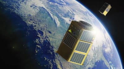
New satellites equipped with Corning’s advanced hyperspectral-imaging technology can detect pipeline leaks and other environmental issues, providing precise monitoring and exploration capabilities for businesses and governments.
Articles: RF & Microwave Electronics
The year 2024 will be full of new satellite manufacturing, launches and operations, with major players like Amazon expected to start full-scale deployment of Project Kuiper and strong demand for low Earth orbit (LEO) satellites driving development and launches from the likes of SpaceX and Telesat among others.

Articles: Photonics/Optics
Scientists led by Nanyang Technological University, Singapore (NTU Singapore) have developed a novel method to produce intense and ultra-fast lasers that holds promise for making precise devices that can speed up how quickly trace amounts of pollutants and hazardous gases can be sniffed out.

Special Reports: Photonics/Optics

Space Technology - January 2024
NASA is making progress in solving some of the most daunting challenges of future space exploration – how to survive the extreme cold of the lunar night, generate oxygen for Mars colonies, and create artificial...Briefs: Materials
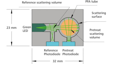
The optical concentration sensor has been demonstrated to effectively measure pretreat concentrations in both still and flowing liquid conditions and is resistant to contamination issues as necessitated by the UWMS.
Briefs: Photonics/Optics
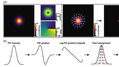
Researchers at Boston University recently developed a novel deblurring algorithm that improves the resolution of images with photon intensity conservation and local linearity.
Briefs: Photonics/Optics
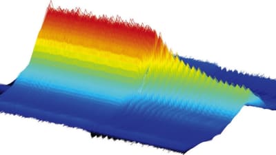
With this new capability, researchers can potentially use frequency combs to better understand the split-second intermediate steps in fast-moving processes ranging from the workings of hypersonic jet engines to the chemical reactions between enzymes that regulate cell growth.
Briefs: Photonics/Optics
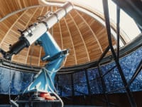
Scientists from the Institute of Geophysics at ETH Zurich, working together with the Swiss Federal Institute of Metrology (METAS), have found an inexpensive method that enables accurate earthquake measurements even on the ocean floor and in less developed countries.

Products: Photonics/Optics
See the new products, including Edmund Optics' new line of ultrafast laser systems; LightPath Technologies, Inc.'s long wave infrared (“LWIR”) microbolometer imaging cores; Metrio Sensors' vertical-cavity surface-emitting laser (VCSEL) array boards; Allied Vision's new Alvium camera series; and more.
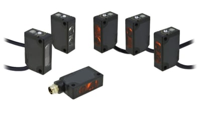
Briefs: Sensors/Data Acquisition
Photoelectric (PE) sensors represent a discrete sensor technology widely used throughout industry. They use the presence or absence of light to provide an on/off output to supervisory automation and monitoring systems, and are often the better choice for sensing manufacturing products.
Blog: Manufacturing & Prototyping
Choosing a present for an engineer is almost as daunting as performing the tasks of an engineer. With that in mind, we here at Tech Briefs aim to make your life easier with regards to the former.

Blog: Photonics/Optics
A new laser-based technique could speed up the discovery of promising metamaterials for real-world applications.
Briefs: Photonics/Optics
Making Satellite, Ground Communication More Effective
Rensselaer Polytechnic Institute’s Moussa N’Gom has devised a method to make communications between satellites and the ground more effective — regardless of the weather.
Briefs: Imaging
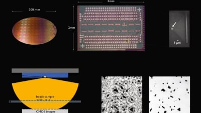
To further shrink electronic devices and to lower energy consumption, the semiconductor industry is interested in using 2D materials but manufacturers need a quick and accurate method for detecting defects in these materials to determine if the material is suitable for device manufacture.
Briefs: Robotics, Automation & Control
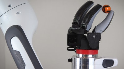
MIT researchers have developed a camera-based touch sensor that is long, curved, and shaped like a human finger. Their device provides high-resolution tactile sensing over a large area. The sensor, called the GelSight Svelte, uses two mirrors to reflect and refract light.
Briefs: Photonics/Optics
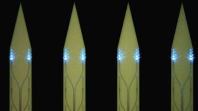
Researchers have developed the world’s smallest LED. It enables the conversion of existing mobile phone cameras into high-resolution microscopes. Smaller than the wavelength of light, the new LED was used to build the world’s smallest holographic microscope.
Products: Electronics & Computers
See the new products, including CamTest TempControl from TRIOPTICS,
Semtech Corporation's Transimpedance Amplifiers, Kaman Precision Products' ThreadChecker, Keysight Technologies' oscilloscopes, and more.
Articles: Materials
Chalcogenide materials have emerged as a disruptive force in the optics industry, significantly enhancing optical performance in response to germanium export constraints. Their exceptional optical properties, adaptability, and precision engineering capabilities position them as invaluable assets for top optical performance.

Application Briefs: Photonics/Optics
Researchers from MIT Lincoln Laboratory and their collaborators at the Massachusetts General Hospital Center for Ultrasound Research and Translation have developed a new medical imaging device: the Noncontact Laser Ultrasound (NCLUS).

Briefs: Photonics/Optics
Researchers have developed a viable dust, water, and ice mitigation optical coating for space flight, aeronautical, and ground applications. The innovation of the LOTUS coating prevents contamination on sensitive surfaces.

Briefs: Photonics/Optics
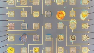
A team of researchers demonstrated the first light-emitting array with 49 different colors on a single chip. This novel optoelectronic device is built on metal-oxide semiconductor capacitors.
Briefs: Lighting
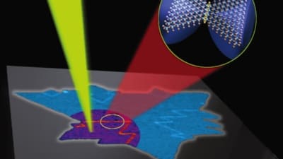
With a new microscopy technique that uses blue light to measure electrons in semiconductors and other nanoscale materials, a team of researchers is opening a new realm of possibilities in the study of these critical components, which can help power devices like mobile phones and laptops.
Briefs: Photonics/Optics
Researchers have outlined a new optical communication protocol that exploits spatial patterns of light for multi-dimensional encoding in a manner that does not require the patterns to be recognized, thus overcoming the prior limitation of modal distortion in noisy channels.

Briefs: Materials
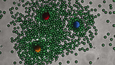
Researchers at the University of California San Diego have developed soft devices containing algae that glow in the dark when experiencing mechanical stress, such as being squished, stretched, twisted, or bent.

Briefs: Photonics/Optics
Researchers from Imperial College London and University College London have demonstrated the first spontaneously self-organizing laser device, which can reconfigure when conditions change.
INSIDER: Photonics/Optics
A collaborative group of researchers has manipulated the behavior of light as if it were under the influence of gravity. The findings, which were published in the...

INSIDER: Photonics/Optics
India's new Center for Programmable Photonics Integrated Circuits and Systems (CPPICS) opened with an inaugural ceremony hosted by the nation's secretary of electronics and information...

Briefs: Photonics/Optics
Touchless switches are an ideal solution for industries such as food, beverage, pharmaceuticals, medical, and chemicals where sanitary design is important. They are also useful for protecting the well-being of users in everyday commercial applications.

Briefs: Imaging
The tool shows promise for imaging brain activity in 3D with high speed and contrast.
Top Stories
 Blog: Robotics, Automation & Control
Aerial Microrobots That Can Match a Bumblebee's Speed
 Blog: Electronics & Computers
Turning Edible Fungi into Organic Memristors
 Blog: Manufacturing & Prototyping
Revolutionizing the Production of Semiconductor Chips
 News: Energy
 INSIDER: Electronics & Computers
World’s Smallest Programmable, Autonomous Robots
 INSIDER: Manufacturing & Prototyping
Webcasts
 On-Demand Webinars: Power
E/E Architecture Redefined: Building Smarter, Safer, and Scalable Vehicles
 Upcoming Webinars: Energy
Hydrogen Engines Are Heating Up for Heavy Duty
 Upcoming Webinars: Electronics & Computers
Advantages of Smart Power Distribution Unit Design for Automotive...
 Upcoming Webinars: Automotive
Quiet, Please: NVH Improvement Opportunities in the Early Design...
 Upcoming Webinars: Power
A FREE Two-Day Event Dedicated to Connected Mobility
 Podcasts: Defense
How Sift's Unified Observability Platform Accelerates Drone Innovation