
A proposal has been made to exploit the special wavelength-dispersive characteristics of devices of the type described in “One-Dimensional Photonic Crystal Superprisms” (NPO-30232) NASA Tech Angle of Incidence Briefs, Vol. 29, No. 4 (April 2005), page 10a. A photonic crystal is an optical component that has a periodic structure comprising two dielectric materials with high dielectric contrast (e.g., a semiconductor and air), with geometrical feature sizes comparable to or smaller than light wavelengths of interest.
Experimental superprisms have been realized as photonic crystals having three-dimensional (3D) structures comprising regions of amorphous Si alternating with regions of SiO2, fabricated in a complex process that included sputtering. A photonic crystal of the type to be exploited according to the present proposal is said to be one-dimensional (1D) because its contrasting dielectric materials would be stacked in parallel planar layers; in other words, there would be spatial periodicity in one dimension only. The processes of designing and fabricating 1D photonic crystal superprisms would be simpler and, hence, would cost less than do those for 3D photonic crystal superprisms. As in 3D structures, 1D photonic crystals may be used in applications such as wavelength-division multiplexing. In the extended-range configuration (see Figure 1), it is also suitable for spectrometry applications.
As an engineered structure or artificially engineered material, a photonic crystal can exhibit optical properties not commonly found in natural substances. Prior research had revealed several classes of photonic crystal structures for which the propagation of electromagnetic radiation is forbidden in certain frequency ranges, denoted photonic bandgaps. It had also been found that in narrow frequency bands just outside the photonic bandgaps, the angular wavelength dispersion of electromagnetic waves propagating in photonic crystal superprisms is much stronger than is the angular wavelength dispersion obtained by use of conventional prisms and diffraction gratings and is highly nonlinear.
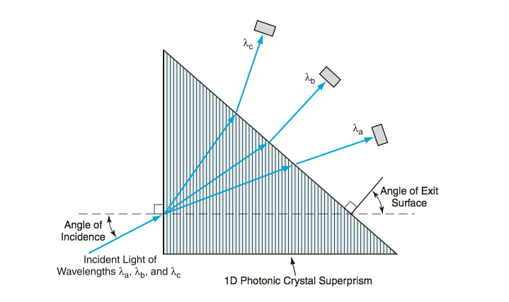
In recent theoretical calculations leading to the present proposal, it was found that in the extended-range configurations, the 1D photonic crystal prism exhibits very strong wavelength dispersion properties over wavelength ranges covering entire photonic bands, rather than at the band edges only. The dependence of angular dispersion as a function of wavelength is also found to be less non-linear. While the wavelength dispersing capability in the extended-range configuration is not as dramatic as in the narrow-range (band-edge only) ultra-refractive configuration, it is still calculated to be over one order of magnitude stronger than that of the conventional prism.
Hence, in designing photonic crystal superprisms to effect wavelength dispersion of polychromatic light, it would be possible to utilize broader wavelength ranges, maintain high transmissivity through use of wavelengths farther from the edges of the photonic bandgaps, take advantage of the reduction in nonlinearity to simplify the positioning of optical components, and take advantage of larger crystal spatial periods to further simplify fabrication. The design parameters that could be varied to obtain the desired properties include the angle of incidence, the angle of the exit surface, and the thicknesses of the layers.
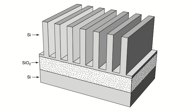
One-dimensional photonic crystal superprisms for visible and infrared wavelengths could be fabricated on semiconductor wafers and, hence, could be integrated monolithically with other miniature optical components. In one example of this approach, a 1D photonic crystal superprism would be fabricated by patterning and anisotropic etching of one of two silicon layers of a silicon-on-insulator substrate (see Figure 2). In this case, the insulator (SiO2) would not only provide structural support, because the index of refraction of SiO2 is lower than that of Si, the SiO2 layer would also act as an optical cladding layer to confine light to the 1D photonic crystal.
This work was done by David Z. Ting of Caltech for NASA’s Jet Propulsion Laboratory. NPO-30594
This Brief includes a Technical Support Package (TSP).
Extended-Range Ultrarefractive 1D Photonic Crystal Prisms
(reference NPO-30594) is currently available for download from the TSP library.
Don't have an account?
Overview
The document is a Technical Support Package from NASA's Jet Propulsion Laboratory (JPL) detailing the innovation of Extended-Range Ultrarefractive 1D Photonic Crystal Prisms, identified by NTR Number 30594. This technology represents a significant advancement in the field of optics, particularly in the manipulation of polychromatic electromagnetic waves.
The core innovation lies in the use of one-dimensional (1D) photonic crystals to create prisms that can effectively separate light into its constituent wavelengths. Unlike traditional prisms that primarily utilize the edges of photonic bands for wavelength dispersion, these 1D photonic crystal prisms leverage the entire transmission bands. This capability allows for broader wavelength ranges, improved optical transmission, and reduced non-linearity, making them more efficient than conventional methods.
The design and fabrication of these prisms are simplified due to their geometry, which permits the use of larger feature sizes in the photonic crystal. This reduction in complexity not only streamlines the manufacturing process but also enhances the tunability of the prism's properties. By adjusting parameters such as incidence angle, exit surface angle, and layer widths, the performance of the prism can be optimized for specific applications.
The document outlines potential applications for these photonic crystal prisms, including dense wavelength division multiplexing (DWDM) and ultra-compact spectrometers. These applications are particularly relevant in telecommunications and analytical instrumentation, where precise wavelength separation is crucial.
Additionally, the Technical Support Package emphasizes the broader implications of this technology beyond aerospace, suggesting its relevance in various scientific and commercial fields. The document is part of NASA's Commercial Technology Program, aimed at disseminating aerospace-related developments with wider technological applications.
For further inquiries or assistance regarding this technology, the document provides contact information for the Innovative Technology Assets Management at JPL.
In summary, the Extended-Range Ultrarefractive 1D Photonic Crystal Prisms represent a novel approach to optical wavelength separation, offering enhanced performance, simplified fabrication, and a wide range of potential applications, marking a significant step forward in photonic technology.