In 1964, NASA’s Electronics Research Center (ERC) opened in Massachusetts, serving to develop the space agency’s in-house expertise in electronics during the Apollo era. The center’s accomplishments include development of a high-frequency (30-GHz) oscillator, a miniaturized tunnel-diode transducer, and a transistor more tolerant of space radiation. Another development was in the area of holography. At the ERC, holography was “used for data storage, and has permitted a remarkable degree of data compression in the storing of star patterns.”
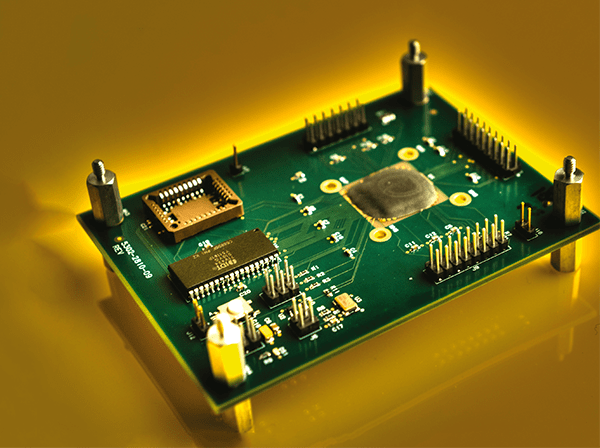
Today, NASA’s research into space electronics has far-reaching applications in commercial industries.
Cooling Integrated Circuits
Future integrated circuitry is expected to look a lot like skyscrapers — units will be stacked on top of one another, and interconnects will link each level to its adjacent neighbors, much like how elevators connect one floor to the next. The problem is how integrated circuit designers can remove heat from these tightly packed 3D chips. The smaller the space between the chips, the harder it is to remove the heat.
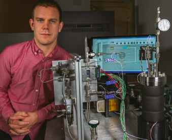
“These 3D-stacked integrated circuits are coming; they will be commercialized. We need to get ahead of the curve when they do become available,” Robinson said.
To make sure NASA benefits from this emerging 3D circuit technology, Robinson and his team have begun investigating a technology that would remove heat by flowing a coolant through embedded channels about the size of a human hair within or between the chips.
In contrast, removing heat in more traditional 2D integrated circuits is significantly different. Designers create a “floor plan,” keeping the heat-generating devices as far apart as possible. The heat travels into the printed circuit board, where it is directed to a clamp in the sidewall of the electronics box, eventually making its way to a box-mounted radiator.
“This approach is not applicable to chip stacks because one or more of the chips in the stack is not in contact with the printed circuit board,” he said. “However, we can remove the heat by flowing a coolant through these tiny, embedded channels.”
Under his research, Robinson is evaluating two-phase flows in miniature channels, with the goal of producing a list of criteria for channel dimensions, flow parameters, and fluid properties that produce gravity insensitivity.
Faster Link Gives Scientists the Speed They Need
For scientists studying the voluminous amounts of data collected daily by NASA’s Soil Moisture Active Passive (SMAP) mission, speed is everything. A new NASA-developed data-transmission technology installed at the U.S. Antarctic Program’s McMurdo Station in Antarctica is giving them the speed they need.
Since SMAP began gathering soil-moisture measurements in the spring, the upgraded McMurdo TDRSS Relay System (MTRS) has transmitted terabytes of data via NASA’s Tracking and Data Relay Satellite System (TDRSS) at a whopping 200 megabits per second (Mbps).
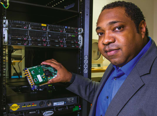
“Not only do they have a lot of data to downlink, the mission’s data also is time-sensitive. We have only 30 minutes to deliver the data from one pass,” he said, adding that MTRS is actually capable of 300 Mbps data-transfer speeds.
As the polar-orbiting SMAP flies over Antarctica, it downlinks roughly 10 gigabytes of data during each pass to an X-band receiver located at the McMurdo Ground Station. A fiber-optic cable carries the data to the MTRS equipment housed 1.5 miles away inside a radome covering the MTRS 4.6-meter antenna dish and the system’s high-speed terminal consisting of two boxes or racks of electronic equipment. Every 12-hour period, the data are transferred to a TDRSS spacecraft that then downlinks the data to NASA’s Space Network ground station at the White Sands Complex, east of Los Cruces, NM, for ultimate delivery to SMAP scientists.
To create the capability, the team upgraded an existing system that Goddard initially developed 15 years ago to demonstrate data transfer from McMurdo to White Sands. The previous incarnation of the system was last used in 2005, and had remained dormant since. Among other issues, the existing equipment fell far short of SMAP’s operational readiness for data transfer and timing.
The team designed, upgraded, and refurbished every aspect of the system. It created the software, custom transceivers, and high-speed computers to produce the fastest data link off the world’s southern-most continent.
3D Printing for Electronics Packaging
For the past two years, the Internal Research and Development, or IRAD, program at NASA Goddard has awarded funding to a small number of researchers who are investigating how the agency might benefit from additive manufacturing or 3D printing. Said NASA Goddard Chief Technologist Peter Hughes, “We’re interested in finding out how this technology can enhance NASA’s ability to create one-of-a-kind instruments and components geared exclusively to studying and operating in space; in other words, improve what we already do well.”
One area that could potentially benefit from 3D manufacturing is electronics, particularly the techniques that technologists use to remove heat from heat-sensitive computer chips. Principal Investigator Jeffrey Didion, a researcher at NASA Goddard, is involved in a comprehensive, multi-year effort to advance electrohydrodynamic (EHD)-based thermal control for removing heat from spacecraft electronics.

Didion is continuing to investigate how he might use additive manufacturing to integrate EHD into the electronics board itself. “What we’d like to do is look at integrating thermal management into a functioning electronics board. In theory, we could do a better job of packaging devices and reducing mass, power consumption, and volume” — a notable endeavor given NASA’s push to reduce instrument size and fly a greater number of lessexpensive CubeSats and other smaller spacecraft.
To that end, Didion has joined forces with NASA Goddard Principal Investigator Beth Paquette, who received IRAD funding to advance a common customizable instrument electronics package called MinE Pack. The device would combine different functions inherent in all instruments — housekeeping, data processing, power, digitization, control and data handling, and amplification — all onto a single 3D chip or stack of chips.
“Our goal is to have all functions packaged into a component that could be plugged into a board or instrument,” Paquette said. “To help us get there, we plan to use additive manufacturing that could print conductors from chip to substrate.”
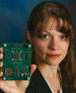
Last year, Paquette focused on advancing MinE Pack’s possible “housekeeping” function using the NASA Goddard-developed “Housekeeping-System-on-a-Chip,” a structured, radiation-hardened application-specific integrated circuit designed to monitor everything from voltages and currents to temperature levels, all while consuming less than half a Watt of power. Working with the chip’s creator, George Suarez, she defined the process for bonding the housekeeping chip onto a printed wiring electronics board.
“The future is looking to additive manufacturing techniques in electronics packaging. This opens up a lot of opportunities for miniaturized packaging, while decreasing the costs of spacecraft electronics,” she said.
Radiation Shielding for Sensitive Circuitry
NASA Goddard Principal Investigator Jean-Marie Lauenstein also is investigating the use of 3D printing to solve another electronics challenge — protecting sensitive circuitry from damage caused by exposure to space radiation.
“Dosages from radiation can degrade performance to the point where the electronics no longer work,” she explained. To protect them, instrument developers currently house sensitive components inside an electronics box made of metal. The thickness of that box depends in part on how much radiation the components are expected to encounter. Although the technique is effective, it “adds a tremendous amount of mass,” she said. Engineers also use “spot shielding,” which usually involves placing a slab of metal over the part.
Lauenstein’s team plans to continue tests to make sure the printed shields can withstand the harsh environmental conditions encountered during launch and in space. So far, Lauenstein is optimistic, believing 3D printing could allow instrument developers in the future to use more state-of-the-art, non-radiation-hardened circuits and rely less on mass-intensive, box-level shielding.
Quantum Computing
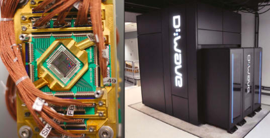
NASA’s Quantum Artificial Intelligence Laboratory (QuAIL) at Ames Research Center in California is the space agency’s hub for an experiment to assess the potential of quantum computers to perform calculations that are difficult or impossible using conventional supercomputers. NASA’s QuAIL team aims to demonstrate that quantum computing and quantum algorithms may someday dramatically improve the agency’s ability to solve difficult optimization problems for missions in aeronautics, Earth and space sciences, and space exploration.
Beginning with the D-Wave Two™ quantum computer, NASA’s QuAIL team is evaluating various quantum computing approaches to help address NASA challenges. Initial work focuses on theoretical and empirical analysis of quantum annealing approaches to difficult optimization problems. The team is also studying how the effects of noise, imprecision in the quantum annealing parameters, and thermal processes affect the efficacy and robustness of quantum annealing approaches to these problems. The team is also developing quantum AI algorithms, problem decomposition and hardware embedding techniques, and quantum-classical hybrid algorithms.

