
An improved method of growing high-quality InAs quantum dots embedded in lattice-matched InGaAs quantum wells on InP substrates has been developed. InAs/InGaAs/InP quantum dot semiconductor lasers fabricated by this method are capable of operating at room temperature at wavelengths ≥1.8 mm. Previously, InAs quantum dot lasers based on InP substrates have been reported only at low temperature of 77 K at a wavelength of 1.9 µm.
In the present method, as in the prior method, one utilizes metal-organic vapor phase epitaxy to grow the aforementioned semiconductor structures. The development of the present method was prompted in part by the observation that when InAs quantum dots are deposited on an InGaAs layer, some of the InAs in the InGaAs layer becomes segregated from the layer and contributes to the formation of the InAs quantum dots. As a result, the quantum dots become highly nonuniform; some even exceed a critical thickness, beyond which they relax.
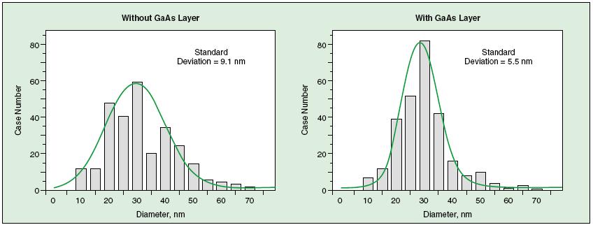
In the present method, one covers the InGaAs layer with a thin layer of GaAs before depositing the InAs quantum dots. The purpose and effect of this thin GaAs layer is to suppress the segregation of InAs from the InGaAs layer, thereby enabling the InAs quantum dots to become nearly uniform (see figure). Devices fabricated by this method have shown near-room-temperature performance.
This work was done by Yueming Qiu and David Uhl of Caltech for NASA's Jet Propulsion Laboratory. NPO-30903
This Brief includes a Technical Support Package (TSP).
(NANO) The way to grow high quality InAs quantum dot active region for mid-infrared (>1.8 micron) semiconductor laser applications
(reference NPO30903) is currently available for download from the TSP library.
Don't have an account?
Overview
The document presents a technical support package from NASA detailing advancements in the growth of high-quality InAs quantum dots (QDs) for mid-infrared semiconductor laser applications, specifically targeting emission wavelengths greater than 1.8 microns. Historically, achieving high-quality InAs QDs with emission wavelengths longer than 1.7 microns has been challenging, with existing reports of InAs QDs and QD lasers operating at 1.9 microns only at low temperatures (77 K).
The research focuses on the deposition of InAs QDs on an InGaAs layer, where it was discovered that the InAs from the InGaAs layer contributes to the formation of the subsequent InAs QDs. This process leads to non-uniformity in the QDs, with some exceeding critical thickness and relaxing, which negatively impacts their performance. To address this issue, the authors propose an innovative solution: covering the underlying InGaAs layer with one or two monolayers (0.3 to 0.6 nm) of GaAs. This approach effectively prevents InAs segregation from the InGaAs layer during the nucleation of InAs QDs.
The results of this method demonstrate excellent size uniformity and strong room temperature luminescence for the InAs QD structures, marking a significant breakthrough in the field. The document emphasizes the importance of embedding InAs QDs within a lattice-matched InGaAs quantum well (QW) on InP substrates to achieve the desired long emission wavelengths.
The motivation behind this research stems from the need to improve the performance of InAs QD lasers, which have been limited by low-temperature operation. By enhancing the size uniformity and luminescence efficiency of InAs QDs, the authors aim to facilitate the development of high-quality QD lasers that can operate at room temperature and achieve longer wavelengths.
Overall, this document outlines a significant advancement in semiconductor laser technology, with potential applications in various fields, including telecommunications and sensing. The innovative techniques described could pave the way for the next generation of mid-infrared lasers, overcoming previous limitations and expanding the capabilities of quantum dot technology.