
A proposed multilayer metal-film/dielectric-plate laminate would serve as a passive radio-frequency (RF) interlayer stripline transition. This device is designed to provide RF coupling from (a) an input transmission line of the stripline type spanning the first through third metal layers, with characteristic impedance Z0s to (b) an intermediate transmission line of the parallel-line type spanning the first through fifth metal layers, with characteristic impedance Z0p ≈ Z0s to (c) an output transmission line of the stripline type spanning the third through fifth metal layers, with characteristic impedance Z0s.
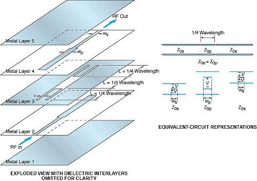
The main advantage of this device lies in its purely planar geometry. Generally, interlayer stripline coupling is achieved by use of vertical probes; that is, through-the-thickness electrical interconnections, which contribute to difficulty of fabrication. The present design provides for RF coupling via the interlayer electromagnetic field, eliminating the need for vertical probes and thereby easing fabrication.
The basic configuration of the device is illustrated in Figure 1. All of the dielectric layers (not shown) between the metal layers are assumed to be of equal thickness h and equal relative permittivity εr. The quarter-wavelength slots in the input and output regions of layer 3 suppress undesired components of interlayer propagation in those regions. Specific dimensions can be altered somewhat (for example, slot lengths can be made to differ slightly from a quarter wavelength) to suit specific applications, without deviating from the overall design concept.
A trial design for an operating frequency of about 1 GHz specifies the following parameters:
- h = 0.125 in. = 3.175 mm
- ωs = 7 mm
- ωp = 15 mm
- L = 60 mm
- t = 15 mm
- εr = 1.1
- Z0s = 61 Ω
- Z0p = 60 Ω
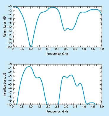
Figure 2 shows return and insertion losses calculated for this design.
This work was done by Ann N. Tulintseff of Caltech for NASA's Jet Propulsion Laboratory. For further information, access the Technical Support Package (TSP) free on-line at www.techbriefs.com under the Electronic Components and Systems category. In accordance with Public Law 96-517, the contractor has elected to retain title to this invention. Inquiries concerning rights for its commercial use should be addressed to
Technology Reporting Office JPL Mail Stop 122-116 4800 Oak Grove Drive Pasadena, CA 91109 (818) 354-2240
Refer to NPO-20115, volume and number of this NASA Tech Briefs issue, and the page number.
This Brief includes a Technical Support Package (TSP).
Interlayer stripline transition
(reference NPO20115) is currently available for download from the TSP library.
Don't have an account?
Overview
The document provides details about two significant engineering and technology expos scheduled for late 1999, aimed at professionals in design, manufacturing, and technology sectors.
The first event is the New England Design & Manufacturing Expo, taking place from September 20-22, 1999, at the Hynes Convention Center in Boston, MA. This expo focuses on the latest products and services that assist engineers in overcoming challenges related to design, prototyping, testing, and production. A highlight of the event is the CAD & Rapid Prototyping Pavilion, which showcases advancements in computer-aided design and rapid prototyping technologies. The expo is colocated with two other significant events: Photonics East, the only optics and photonics exhibition in the Northeast, and Electronic Imaging International, recognized as the East Coast’s premier annual imaging expo.
The second event is Technology 2009, scheduled for November 1-3, 1999, at the Fontainebleau Hilton in Miami Beach, Florida. This is the tenth annual "Engineering Innovation Show," which serves as a major platform for showcasing new and next-generation technologies available for licensing and commercial development. It is colocated with the Southeast Design & Manufacturing Expo, which specifically targets the high-tech corridor in the Southeast, and the Small Business Tech Expo, which focuses on resources and technologies for launching new products and partnerships.
Both expos offer free admission to hundreds of exhibits, providing attendees with opportunities to explore cutting-edge engineering solutions, product ideas, and potential business partnerships. The document encourages professionals to plan their attendance at these events to gain insights into the latest industry trends and innovations.
For more information, attendees are directed to contact Stephanie Torchinsky at the provided phone number or email, and they can also visit the website www.techeast.net for further details. The expos are sponsored by Tech East, emphasizing their role as a vital source for engineering solutions and business opportunities in the rapidly evolving technology landscape.