
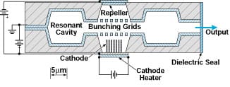
An array of monolithically fabricated nanoklystrons has been proposed as a frequency-agile and/or redundant source of electromagnetic radiation at frequencies ranging from about 0.3 to about 3 THz. Each nanoklystron would, as its name suggests, be a very small klystron. Like other klystrons, a nanoklystron would operate at a frequency determined primarily by the dimensions of its resonant cavity and the spacing of its electron-bunching grids, with some dependence on applied voltages. An individual nanoklystron could be fabricated in top and bottom halves from silicon wafers and would contain an integral output waveguide and feed horn (see Figure 1). In typical operation, a nanoklystron without a mechanical tuner would generate power only at a fixed frequency. Thus, frequency agility and/or redundancy could be obtained by incorporating into the array multiple nanoklystrons that are pretuned to generate signals at all required frequencies.
This work was done by Peter Siegel of Caltech for NASA's Jet Propulsion Laboratory. For further information, access the Technical Support Package (TSP) free on-line at www.nasatech.com/tsp under the Electronics & Computers category.
In accordance with Public Law 96-517, the contractor has elected to retain title to this invention. Inquiries concerning rights for its commercial use should be addressed to
Intellectual Property group
JPL
Mail Stop 202-233
4800 Oak Grove Drive
Pasadena, CA 91109
(818) 354-2240
Refer to NPO-21033, volume and number of this NASA Tech Briefs issue, and the page number.
This Brief includes a Technical Support Package (TSP).
Array of Nanoklystrons for Frequency Agility or Redundancy
(reference NPO-21033) is currently available for download from the TSP library.
Don't have an account?
Overview
The document presents a technical overview of an innovative array of nanoklystrons developed by Peter H. Siegel at NASA's Jet Propulsion Laboratory (JPL). The primary focus is on enhancing frequency agility and redundancy in terahertz (THz) applications. Nanoklystrons are miniature versions of conventional klystrons, designed to operate efficiently at submillimeter wavelengths, making them valuable for various advanced technological applications.
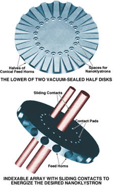
The proposed design involves fabricating multiple nanoklystrons on a single silicon wafer, which is compatible with the industry standard diameter of 8 inches (approximately 20 cm). This approach allows for the production of thousands of nanoklystrons in a single run, each tailored to operate at specific frequencies. The document outlines the fabrication process, which includes forming contact pads on the top and bottom of a disk that houses the nanoklystrons. These pads enable power supply to individual klystrons, while registration notches facilitate precise alignment during operation.
A key feature of the design is the ability to rotate the disk to select a specific nanoklystron, bringing it into the proper position for output coupling. This mechanism allows for quick and efficient switching between different frequencies, addressing the challenge of frequency agility in THz applications. The document emphasizes that by increasing the diameter of the host wafer, a broader range of frequencies can be targeted, all while maintaining similar output beam properties.
The work is positioned as a significant advancement in the field of electromagnetic technology, particularly for applications requiring high-frequency signals. The compact nature of the nanoklystron array not only enhances performance but also offers redundancy, ensuring reliability in critical systems.
The document concludes with a note on the intellectual property rights associated with the invention, indicating that the contractor retains title to the invention under Public Law 96-517. Inquiries regarding commercial use are directed to the Technology Reporting Office at JPL.
Overall, this report highlights the potential of nanoklystrons in revolutionizing THz technology, providing a pathway for more versatile and efficient electromagnetic systems.