
A suite of electronic test equipment has been developed for use in the measurement of key electrical characteristics of advanced, high-speed integrated circuits for communications, radar, digital networks, imaging systems, and other applications. More specifically, the test equipment is designed to enable the determination of noise figures and of scattering parameters (commonly denoted "S" parameters) at frequencies up to 220 GHz. The equipment includes (1) test sets that are basically extended versions of commercial network analyzers that, heretofore, have been functional up to 110 GHz; (2) recently developed millimeter-wavelength-signal probes that make it possible to take accurate on-wafer measurements; and (3) an amplifier-based solid-state noise source.
In commercial network analyzers, coverage of frequencies from 50 to 110 GHz is typically accomplished by use of frequency-extension modules that contain multipliers and harmonic mixers. The basic frequency-extender concept is readily applicable to frequencies up to 220 GHz and possibly as high as 325 GHz. Accordingly, the present 220-GHz test sets were developed on the basis of this concept, and were designed to satisfy the following criteria:
- The configuration of the frequency-extension modules must follow accepted industry practice and must be such that one can obtain S11 and S21 by use of a minimal test system and can obtain all four "S" parameters (S11, S12, S21, and S22) by use of a complete test system.
- The intermediate frequency (IF) use in the test set must be compatible with the most common commercial open-architecture network analyzers.
- The signal radio frequency (RF) and the local-oscillator (LO) drive requirements must be chosen with cost acknowledged as a major design constraint.
Heretofore, in order to measure the electrical characteristics of circuits at frequencies above 100 GHz, it has been necessary to package the circuits into waveguide blocks; this practice is slow and cumbersome, and often does not yield true circuit performance. In contrast, by enabling accurate on-wafer measurements, the recently developed signal probes included in the present test equipment can be expected to foster commercialization by making it possible to characterize circuits accurately, in rapid succession, at relatively low cost.
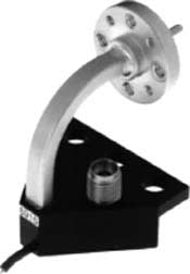
The figure depicts one in a line of coplanar probes designed for testing millimeter wave circuits. The probe tips, made of beryllium-copper, are individually spring-loaded for reliable connections even to nonplanar circuit structures. A bias T is included to provide current (up to 1.5 A) to the circuit under test and includes loss elements to absorb signals below the waveguide cutoff frequency (115 GHz in this case), where the waveguide becomes highly reflective. Special miniaturized coplanar calibration substrates have been developed for use with this and the other probes.
In tests of a receiver circuit, it was found to be cumbersome to perform noise measurements by use of alternate hot and cold loads in front of a feed horn attached to a wafer probe. Therefore, a transfer standard was constructed: An amplifier with a frequency range of 150 to 190 was packaged into a waveguide block. With its input terminated and its output attenuated to provide a stable output impedance, the amplifier proved to be an ideal semiconductor noise source with an excess-noise ratio of 10 dB. The estimated error in the noise figure measurement is less than 1 dB.
The use of the amplifier as a noise source makes it possible to use a commercial noise-figure meter as an IF processor. This, in turn, enables optimization of biases of circuits under test. In contrast, optimization of bias during testing with hot and cold loads has proved to be a tedious task that has yielded inaccurate results.
This work was done by Todd Gaier and Lorene Samoska of Caltech, Charles Oleson of Oleson Microwave Labs, and Greg Boll of GBB Industries for NASA's Jet Propulsion Laboratory. For further information, access the Technical Support Package (TSP) free on-line at www.nasatech.com/tsp under the Electronics & Computers category.
NPO-20760
This Brief includes a Technical Support Package (TSP).
Equipment for On-Wafer Testing at Frequencies Up to 220 GHz
(reference NPO-20760) is currently available for download from the TSP library.
Don't have an account?
Overview
The document outlines the development of advanced electronic test equipment designed for on-wafer testing of high-speed integrated circuits at frequencies up to 220 GHz, conducted by NASA's Jet Propulsion Laboratory (JPL). This innovative technology aims to enhance the measurement of key electrical characteristics in circuits used for communications, radar, digital networks, and imaging systems.
The equipment includes several key components: extended versions of commercial network analyzers, millimeter-wavelength-signal probes for accurate on-wafer measurements, and an amplifier-based solid-state noise source. Traditional methods for measuring electrical characteristics at frequencies above 100 GHz often required packaging circuits into waveguide blocks, a process that was slow and cumbersome, potentially leading to inaccurate results. The new on-wafer measurement capabilities allow for rapid and accurate characterization of circuits, facilitating commercialization and development in high-frequency applications.
The test sets are designed to meet specific criteria, including compatibility with existing commercial network analyzers and cost-effective design considerations. They enable the determination of noise figures and scattering parameters (S-parameters) with minimal test systems, allowing for efficient data collection and analysis. The use of a solid-state noise source simplifies the process of optimizing circuit biases, which has traditionally been a tedious task when using hot and cold loads for testing.
The document highlights the collaborative efforts of researchers Todd Gaier, Lorene Samoska, Charles Oleson, and Greg Boll in developing this technology for NASA. The advancements presented in this report are expected to significantly improve the testing and characterization of high-speed circuits, making it easier to develop and optimize technologies for various applications.
In summary, this document presents a significant leap forward in the field of high-frequency testing, showcasing a suite of equipment that enhances the accuracy and efficiency of on-wafer measurements at frequencies up to 220 GHz. This development not only streamlines the testing process but also supports the ongoing advancement of integrated circuits in critical technological domains.