
A commercial scanning imaging white-light interferometer designed for measuring surface profiles of stationary objects has been modified into an interferometric instrument for imaging vibrating microelectromechanical structures. The modified instrument operates in a stroboscopic mode, generating a set of interferograms at a selected instant in the vibrational cycle. A number of sets of interferograms can be acquired at different instants of time corresponding to small increments of phase through the vibrational cycle so that the resulting collection of interferograms shows how the shape of the vibrating surface changes during the cycle; thus, the interferograms yield information on the shape and amplitude of the vibrational mode or modes.
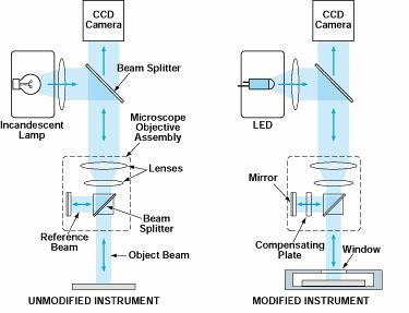
The figure schematically illustrates the unmodified and modified versions of the instrument. The magnified image of the specimen is brought to focus in a charge-coupled-device (CCD) camera oriented along a main (vertical) optical axis. In the unmodified instrument, an incandescent lamp generates white light, which is reflected down along the main optical axis by a beam splitter. The microscope objective assembly contains another beam splitter, which divides the illumination into two beams: a reference beam sideways to the main optical axis and an object beam, which continues down along the main optical axis, through the objective lenses, and onto the specimen.
The reference beam is reflected from a flat mirror, then reflected from the beam splitter in the objective assembly back up the main optical axis toward the camera. The object beam is reflected from the specimen, passes up through the beam splitter and the lenses in the objective assembly, and into the camera. Interference between the object and reference beams forms the desired interference pattern on the focal plane of the camera.
The specimen is moved along the main optical axis, passing through the position of zero optical-path-length difference. CCD outputs representing interferograms are acquired and digitized at various increments of optical-path-length difference. Then by use of special-purpose software, the digital interferograms are used to compute the surface profile of the specimen. The unmodified instrument cannot be used to obtain the surface profile of a vibrating specimen because the vibration blurs the interference patterns.
In the modified instrument, the incandescent lamp is replaced by an ultrabright light-emitting diode (LED), which can be driven by pulses at a repetition rate up to 2 MHz. The pulse generator that drives the LED is synchronized to the function generator that drives the vibrations of the specimen. The phase-offset capability of the function generator is used to select the increments of phase for acquiring sets of interferograms.
Because of the viscous drag, many microelectromechanical structures do not vibrate in air at atmospheric pressure. Therefore, in the modified instrument, the specimen is mounted in a small vacuum chamber and observed through a window. To compensate for the optical path length through the window, the modified instrument includes a plate of the same optical thickness as that of the window inserted in path of the reference beam.
With the modified instrument, vibrational displacements along the main optical axis can be measured with resolutions of the order of nanometers. The only fundamental limitation of the modified instrument lies in the competing requirements for stroboscopic illumination: One must generate enough luminous energy during each pulse to obtain an image, while keeping the pulse short enough, to prevent motion blur of the image. "Short enough" as used here is defined with respect to the amplitude and frequency of the vibration and means, specifically, that the displacement during the pulse must be no more than about 1/20 of the wavelength of the light from the LED.
This work was done by Roman Gutierrez, Kirill Shcheglov, and Tony K. Tang of Caltech for NASA's Jet Propulsion Laboratory. For further information, access the Technical Support Package (TSP) free on-line at www.nasatech.com/tsp under the Physical Sciences category. NPO-20177
This Brief includes a Technical Support Package (TSP).
Interferometric System Images Small Vibrating Structures
(reference NPO-20177) is currently available for download from the TSP library.
Don't have an account?
Overview
The document outlines a significant advancement in interferometric imaging technology, specifically focusing on the modification of a commercial scanning imaging white-light interferometer to enable the imaging of vibrating micro-electromechanical systems (MEMS). The original instrument was designed for measuring surface profiles of stationary objects, but its limitations in capturing dynamic structures prompted the need for modification.
The modified instrument operates in a stroboscopic mode, allowing it to generate a series of interferograms at specific instants during the vibration cycle of the specimen. This capability enables the collection of data that illustrates how the shape of the vibrating surface changes over time, providing critical information on vibrational mode shapes and amplitudes.
Key modifications include replacing the incandescent light source with an ultra-bright light-emitting diode (LED) capable of being modulated at high frequencies (up to 2 MHz). This LED is synchronized with a function generator that drives the vibrations of the specimen, allowing for precise phase-offset control during data acquisition. Additionally, a small vacuum chamber was introduced to minimize viscous drag effects that could hinder the vibration of MEMS structures, and a compensating glass plate was added to the reference arm of the interferometer to correct for image degradation caused by the viewport glass of the chamber.
The document highlights the fundamental limitations of the modified instrument, particularly regarding the brightness of light sources and their modulation capabilities. As vibration amplitudes increase, the duty cycle of the light source must be shortened to prevent blurring of the interference patterns. The current setup allows for a maximum vibration amplitude of about 2 pm, but the use of advanced light sources could potentially increase this limit to 20-50 pm, making the instrument suitable for a wider range of MEMS applications.
Overall, this innovation represents a significant leap in the ability to characterize and analyze the dynamic behavior of MEMS devices, providing unparalleled vertical resolution in the nanometer range over a field of view of several millimeters. The document emphasizes the importance of this technology for advancing the understanding and development of microstructures in various applications.