
A recently proposed boundary condition for atomistic computational modeling of semiconductor nanostructures (particularly, quantum dots) is an improved alternative to two prior such boundary conditions. As explained below, this boundary condition helps to reduce the amount of computation while maintaining accuracy.
The electronic properties of semiconductor nanostructures (hereafter called "nanodevices") are already utilized in sensors, lasers, memory circuits, and electro-optical and optoelectronic devices. The electronic properties of a nanodevice are sensitive to numerous parameters, including those pertaining to sizes, shapes, alloy compositions, and interfaces between different materials. Atomistic computational simulation of a nanodevice can help in the selection of optimal parameters in the huge design space inhabited by the parameters. However, until now, the computational burden posed by the large numbers of atoms in a nanodevice has made it necessary to limit computational modeling to a semi-classical, continuum approximation. The purpose served by the present boundary condition (and by the two prior boundary conditions with which the present boundary condition is compared) is to enable truncation of the simulation domain at an artificial boundary surface so that the domain can be made small enough that atomistic computational simulation becomes practical.
 The truncation problem can be summarized as follows: Whereas, as its name suggests, a nanodevice can have characteristic dimensions of the order of nanometers, it is typically embedded within a larger semiconductor structure having characteristic dimensions of the order of micrometers. Therefore, in the absence of a means of truncation, the simulation domain must typically encompass all of the atoms contained within a micrometer-sized region. The key to truncation lies in recognition that a smaller electronically active region is defined by localization of the electron density in and near a potential well established by the energy-band offset between two adjacent semiconductor materials. However, without a proper boundary condition, simply drawing an artificial boundary surface around the electronically active region results in many spurious quantum states associated with dangling interatomic bonds at the boundary surface.
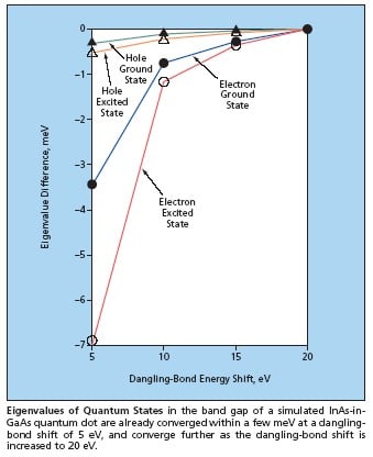
The present boundary condition effectively eliminates the spurious surface quantum states by artificially shifting their energy levels well above the energy band of interest, as though the dangling bonds were passivated by high-energy molecules. The size of the dangling-bond energy shift is not critical, as long as it suffices to remove all spurious quantum states from the semiconductor band gap in the electronically active region of interest. For example, in the case of an InAs self-assembled quantum dot embedded in GaAs, a shift of 5 eV is sufficient to remove the spurious states and make electron and hole energies converge to within a few meV (see figure).
The present boundary condition is a refined version of one of the two prior boundary conditions in which the orbital energies of surface atoms are raised. Whereas the prior boundary condition does not differentiate among such details of the surface atoms as the numbers and directions of their dangling bonds, the present boundary condition does. The present boundary condition is more physically realistic because, unlike in the prior boundary condition, the connected-bond energy of the surface atoms is kept unchanged and, hence, there is no extra energy penalty for electrons to occupy the connected bonds of surface atoms. The other prior boundary condition is a periodic one and, hence, not well suited to modeling a nanodevice that has an irregular shape or is subjected to a nonperiodic externally applied potential.
This work was done by Seungwon Lee, Fabiano Oyafuso, Paul von Allmen, and Gerhard Klimeck of Caltech for NASA's Jet Propulsion Laboratory. For further information, access the Technical Support Package (TSP) free on-line at www.techbriefs.com/tsp under the Physical Sciences category. NPO-41155
This Brief includes a Technical Support Package (TSP).
Boundary Condition for Modeling Semiconductor Nanostructures
(reference NPO-41155) is currently available for download from the TSP library.
Don't have an account?
Overview
The document is a Technical Support Package from NASA's Jet Propulsion Laboratory (JPL) concerning the innovative boundary condition for modeling semiconductor nanostructures, identified by NTR Number: 41155. This work is part of NASA's Commercial Technology Program, aimed at disseminating aerospace-related developments with potential wider technological, scientific, or commercial applications.
The primary focus of the document is on a proposed boundary condition that addresses the challenges associated with dangling-bond energies in semiconductor nanostructures. These dangling bonds can introduce spurious surface states that complicate the band structure of the materials being modeled. The innovative boundary condition effectively shifts these dangling-bond energies away from the energy region of interest, simulating a passivation effect as if they were treated with high-energy molecules. This approach allows for a cleaner and more accurate representation of the band structure, free from the interference of unwanted surface states.
The development of this boundary condition has been documented in a peer-reviewed journal, specifically in "Physical Review B," volume 69, article 045316, published in 2004. This publication underscores the scientific rigor and validation of the proposed method, indicating its relevance and applicability in the field of semiconductor physics.
The Technical Support Package also emphasizes the broader implications of this research, suggesting that advancements in modeling semiconductor nanostructures can lead to significant improvements in various technological domains, including electronics, photonics, and materials science. The document encourages further exploration of related research and technology through the NASA Scientific and Technical Information (STI) Program Office, providing contact details for additional assistance.
Overall, this document serves as a resource for researchers and industry professionals interested in semiconductor modeling, offering insights into innovative techniques that enhance the accuracy and reliability of simulations. It reflects NASA's commitment to fostering innovation and collaboration in technology development, with the potential for applications that extend beyond aerospace into various sectors of science and industry.