
Semiconductor electron-spin filters of a proposed type would be based on the Rashba effect, which is described briefly below. Electron-spin filters — more precisely, sources of spin-polarized electron currents — have been sought for research on, and development of, the emerging technological discipline of spintronics (spin-based electronics). There have been a number of successful demonstrations of injection of spin-polarized electrons from diluted magnetic semiconductors and from ferromagnetic metals into nonmagnetic semiconductors. In contrast, a device according to the proposal would be made from nonmagnetic semiconductor materials and would function without an applied magnetic field.
The Rashba effect, named after one of its discoverers, is an energy splitting, of what would otherwise be degenerate quantum states, caused by a spin-orbit interaction in conjunction with a structural-inversion asymmetry in the presence of interfacial electric fields in a semiconductor heterostructure.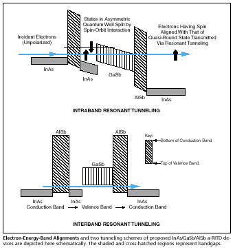 The magnitude of the energy split is proportional to the electron wave number. The present proposal evolved from recent theoretical studies that suggested the possibility of devices in which electron energy states would be split by the Rashba effect and spin-polarized currents would be extracted by resonant quantum-mechanical tunneling. Accordingly, a device according to the proposal would be denoted an asymmetric resonant interband tunneling diode [a-RITD]. An a-RITD could be implemented in a variety of forms, the form favored in the proposal being a double-barrier heterostructure containing an asymmetric quantum well.
It is envisioned that a-RITDs would be designed and fabricated in the InAs/GaSb/AlSb material system for several reasons: Heterostructures in this material system are strong candidates for pronounced Rashba spin splitting because InAs and GaSb exhibit large spin-orbit interactions and because both InAs and GaSb would be available for the construction of highly asymmetric quantum wells. This material system affords a variety of energy-band alignments that can be exploited to obtain resonant tunneling and other desired effects. The no-common-atom InAs/GaSb and InAs/AlSb interfaces would present opportunities for engineering interface potentials for optimizing Rashba spin splitting.
More specifically, a device of this type would comprise an asymmetric composite InAs-GaSb well, sandwiched between AlSb barriers and InAs electrodes. Unpolarized electrons from the conduction band of an InAs emitter electrode would tunnel rapidly through one AlSb barrier and through an asymmetric InAs-GaSb quantum well, where Rashba spin splitting would occur; they would then tunnel through the other AlSb barrier into the conduction band of an InAs collector electrode. With appropriately chosen thicknesses of layers, this device could be made to operate in either of two regimes (see figure):
- Under low bias, in a resonant-interband-tunneling regime, in which electrons would traverse valence subband states in GaSb or
- Under moderate bias, in an intrabandresonant-tunneling regime, in which electrons would traverse conduction subband states in InAs. Computational simulations have led to an expectation that the interband regime would yield better performance.
This work was done by David Z.-Y. Ting, Xavier Cartoixà, and Thomas C. McGill of Caltech; Jeong S. Moon, David H. Chow, and Joel N. Schulman of HRL Laboratories, LLC; and Darryl L. Smith of Los Alamos National Laboratory for NASA's Jet Propulsion Laboratory. For further information, access the Technical Support Package (TSP) free on-line at www.techbriefs.com/tsp under the Physical Sciences category. In accordance with Public Law 96-517, the contractor has elected to retain title to this invention. Inquiries concerning rights for its commercial use should be addressed to: Innovative Technology Assets Management Refer to NPO-30635, volume and number of this NASA Tech Briefs issue, and the page number.
JPL
Mail Stop 202-233
4800 Oak Grove Drive
Pasadena, CA 91109-8099
(818) 354-2240
E-mail:
This Brief includes a Technical Support Package (TSP).
Electron-Spin Filters Based on the Rasba Effect
(reference NPO-30635) is currently available for download from the TSP library.
Don't have an account?
Overview
The document is a technical support package from NASA's Jet Propulsion Laboratory, focusing on advancements in spintronics, particularly the development of electron-spin filters based on the Rashba effect. It discusses the concept of a resonant tunneling spin pump, which aims to create an efficient source of spin-polarized currents, a key area of research in spin-based electronics.
The resonant tunneling spin pump is proposed as a device structure that can achieve high polarization of electron spins through resonant tunneling mechanisms. The theoretical calculations presented indicate that the polarization current (P_J) can exceed 1000, although the document emphasizes that while P_J is significant, it is not the sole metric of interest. The critical factor is the ability to inject polarized carriers quickly enough to maintain polarization in the source materials, which is influenced by the spin relaxation time.
The document highlights that the spin pump's performance is less sensitive to the Fermi level position compared to other spin filtering methods, such as the aRITD (asymmetric resonant interband tunneling device) spin filter. Proposed device structures include the aRITD and a triple-barrier spin blockade structure, both of which are designed to enhance the efficiency of spin injection.
Temperature plays a crucial role in device performance, with preliminary calculations suggesting that lower temperatures lead to better outcomes due to increased carrier mobility. High mobility in both the emitter and collector regions is deemed essential for optimal operation, with reported mobilities of InAs channels reaching 25,000 cm²/Vs at room temperature and 460,000 cm²/Vs at 4.2K.
The document also notes ongoing discussions with HRL Laboratories for the experimental realization of these concepts, supported by funding from the DARPA SpinS program. Overall, the technical support package provides a comprehensive overview of the current state of research in spintronics, emphasizing the potential of resonant tunneling mechanisms to advance the field of spin-based electronics and their applications in various technological domains.