
Experiments have shown that with suitable choices of critical dimensions, planar arrays of bundles of carbon nanotubes (see figure) can serve as high-current-density field emitter (cold-cathode) electron sources. Whereas some hot-cathode electron sources must be operated at supply potentials of thousands of volts, these cold-cathode sources generate comparable current densities when operated at tens of volts. Consequently, arrays of bundles of carbon nanotubes might prove useful as cold-cathode sources in miniature, lightweight electron-beam devices (e.g., nanoklystrons) soon to be developed.
Prior to the experiments, all reported efforts to develop carbon- nanotube-based field-emission sources had yielded low current densities — from a few hundred microamperes to a few hundred milliamperes per square centimeter. An electrostatic screening effect, in which taller nanotubes screen the shorter ones from participating in field emission, was conjectured to be what restricts the emission of electrons to such low levels. It was further conjectured that the screening effect could be reduced and thus emission levels increased by increasing the spacing between nanotubes to at least by a factor of one to two times the height of the nanotubes. While this change might increase the emission from individual nanotubes, it would decrease the number of nanotubes per unit area and thereby reduce the total possible emission current. Therefore, to maximize the area-averaged current density, it would be necessary to find an optimum combination of nanotube spacing and nanotube height.
The present concept of using an array of bundles of nanotubes arises partly from the concept of optimizing the spacing and height of field emitters. It also arises partly from the idea that single nanotubes may have short lifetimes as field emitters, whereas bundles of nanotubes could afford redundancy so that the loss of a single nanotube would not significantly reduce the overall field emission.
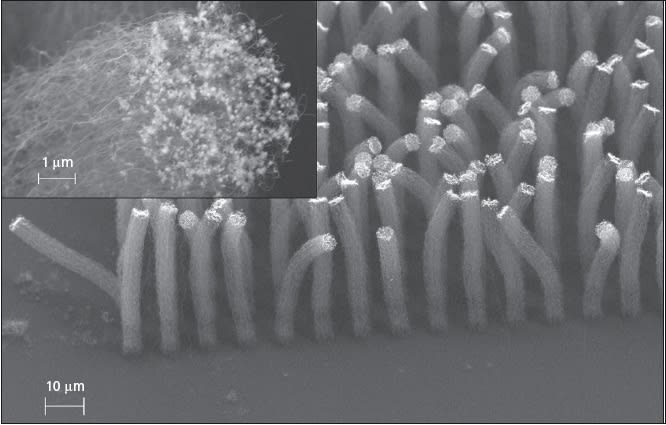
In preparation for the experiments, planar arrays of bundles of carbon nanotubes having various bundle diameters, bundle heights, and bundle spacings were fabricated. The fabrication process can be summarized as follows: Electron-beam lithography was used to form planar arrays of iron dots having various thicknesses and having diameters and inter-dot spacings corresponding to the desired diameters and spacings of the carbon-nanotube bundles. The dots served as catalysts for the growth of carbon nanotubes: Bundles of multi-walled 20-nm-diameter carbon nanotubes were grown on the iron dots by chemical vapor deposition. The average height of the bundles was 70 ± 2μm. The heights of the bundles were found to depend on the thicknesses of the iron dots. The tallest bundles (112 μm high) were found on iron dots 8 μm thick.
In the experiments, field emission from these arrays was measured in a vacuum chamber by use of a 100-μm-diameter probe anode. The highest nondestructive area-averaged current densities (about 1.5 to 1.8 A/cm2) were observed on arrays of bundles of 1- to 2-μm diameter and spacings of 5 μm at an applied electric field of about 4.5 V/μm.
This work was done by Harish Manohara and Michael Bronkowski of Caltech for NASA’s Jet Propulsion Laboratory. For further information, access the Technical Support Package (TSP) free on-line at www.techbriefs.com/tsp under the Physical Sciences category.
In accordance with Public Law 96-517, the contractor has elected to retain title to this invention. Inquiries concerning rights for its commercial use should be addressed to:
Innovative Technology Assets Management
JPL
Mail Stop 202-233
4800 Oak Grove Drive
Pasadena, CA 91109-8099
(818) 354-2240
E-mail: This email address is being protected from spambots. You need JavaScript enabled to view it.
Refer to NPO-40817, volume and number of this NASA Tech Briefs issue, and the page number.
This Brief includes a Technical Support Package (TSP).
Arrays of Bundles of Carbon Nanotubes as Field Emitters
(reference NPO-40817) is currently available for download from the TSP library.
Don't have an account?
Overview
The document is a Technical Support Package from NASA's Jet Propulsion Laboratory (JPL) detailing research on "Arrays of Bundles of Carbon Nanotubes as Field Emitters," identified by NTR Number: 40817. It discusses the innovative use of carbon nanotube bundles to create high current density field emitters, which have potential applications in various technological and scientific fields, particularly in aerospace.
The research focuses on the performance of carbon nanotube bundles in field emission applications. It presents experimental findings that challenge previous modeling conclusions, indicating that bundles of carbon nanotubes behave differently than individual nanotubes. The study tested various configurations of bundle diameters (0.2, 0.5, 1, 2, and 5 microns) and inter-bundle spacings (100, 50, 20, 10, 5, and 2 microns). The results consistently showed that the optimal combination for high field emission was bundles with diameters of 1 micron and 2 microns, spaced 5 microns and 10 microns apart.
The document emphasizes the significance of these findings in advancing the understanding of carbon nanotube behavior in field emission contexts. It suggests that the unique properties of bundled nanotubes can lead to improved performance in applications requiring high current densities, which is crucial for the development of efficient electronic devices and systems.
Additionally, the Technical Support Package serves as a resource for those interested in the commercial and scientific implications of this research. It is part of NASA's Commercial Technology Program, aimed at disseminating aerospace-related developments that have broader technological applications. The document also provides contact information for further inquiries, emphasizing JPL's commitment to innovation and collaboration in technology transfer.
In summary, this document outlines groundbreaking research on carbon nanotube bundles as field emitters, presenting experimental results that highlight their potential advantages over individual nanotubes. It serves as a valuable resource for understanding the implications of this technology in various fields, particularly in enhancing electronic devices and systems.