
We’ve come a long way since Alexander Graham Bell’s famous words, “Mr. Watson, come here” were spoken and the telephone was born. The simplicity of use of today’s smartphones, tablets, and similar smart devices belies the underlying complexity of creating a device that can connect virtually anywhere, at anytime. While there are other consumer electronic devices that have increased in complexity and capability, the majority of the smartphone’s complex structure is completely hidden from the user. At the same time, “when can I upgrade” is a common mantra of users. The fast-paced and high-volume production required in this environment continues to add complexity to mobile device testing, and has necessitated the rethinking of traditional test methods.
Market Forces
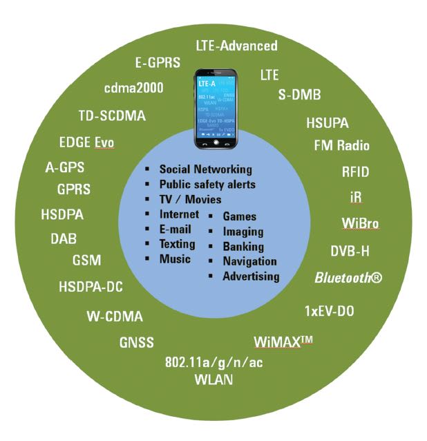
Technology Evolution
Unknown to the average consumer is the evolution of RF technology that has occurred to ensure these devices meet the service expectations of today’s smartphone user (see Figure 2). Today, LTE (Long Term Evolution) – Advanced Carrier Aggregation is the latest technology evolution to create a higher bandwidth pipe between the Internet, or “cloud,” and mobile devices (see Figure 3). This technology allows a service provider to take smaller chunks of their available spectrum and aggregate them into a wider bandwidth channel. LTE-Advanced allows up to five 20- MHz chunks to create an effective 100- MHz channel.
New Testing Needs

Conformance testing ensures that the phone design conforms to the standards for which it was designed. This testing is performed using specialized conformance and pre-conformance test equipment at various stages throughout the design process to ensure any issues are uncovered and addressed early. When the design is done, the phone will typically be certified by a third party as meeting the required standards.
With conformance testing completed, the testing required in manufacturing is focused on two key areas: 1) final device calibration and 2) device verification. These tests are done over a range of power settings and channel configurations for a limited set of key items:

- Channel power – Confirms that the device under test (DUT) has accurate power control.
- Occupied bandwidth – Ensures that the transmission bandwidth of the DUT is within limits.
- Adjacent channel leakage power ratio (aka ACP, ACLR) – Verifies that the DUT does not cause interference to adjacent channels.
- Modulation analysis – Measures parameters, such as error vector magnitude (EVM), to ensure that the signal quality from the DUT meets the standards required for the format(s) in the DUT.
Each of these tests, while not timeconsuming to perform individually, add up when you multiply them by the number of formats and channels (or bands) that must be tested. Using the latest nonsignaling manufacturing test process (see Figure 4), almost all of the overhead associated with establishing the call and making mode changes based on commands from the base station (BTS) is eliminated. Compared to prior testing techniques, the time savings has enabled more complex devices to be tested with minimal impact to production volume. Another benefit of non-signaling test is that it requires a far less expensive piece of test equipment since there is no need to duplicate the functionality of a BTS.
Testing the new functionality of phones, such as Bluetooth® and WLAN, also impacts the duration of testing. Separate measurement applications allow manufacturers to select the modules they need to efficiently test just the functionality necessary. Measurement applications can easily be added in the future as test needs grow.
To ensure testing efficiency, any time not devoted to testing must be minimized or eliminated. Non-signaling test solutions with technology-tailored applications offering single acquisition multiple measurement (SAMM) capability help ensure this goal is achieved. There is one key requirement of non-signaling test: it requires direct control of the DUT.

Solution Longevity
As devices continue to advance with such techniques as carrier aggregation for LTE-Advanced and added formats, such as Wireless LAN (WLAN), Bluetooth, and GNSS receivers, testing challenges continue to grow. New fast-sequenced testing techniques promise to minimize the growth of, or even reduce, test times by loading more complex test routines into the DUTs and capturing them quickly with a high-speed tester. In addition, testing multiple carriers, either sequentially or in parallel, and testing multiple inputmultiple output (MIMO) devices continues to challenge manufacturers striving to get high volumes of quality products out the door. Throughout these changes, smart-device manufacturers will continue to be forced to meet ever-tougher goals and tighter schedules.
To do this effectively in the future, manufacturers must be able to depend on testing solutions that are scalable and provide the speed, accuracy, and density (number of equivalent testers in a given footprint) to ramp-up new product production quickly and cost effectively at full volume. Other desirable test set solution characteristics include raw speed and advanced test sequencing capability.

Conclusion
Just as today’s smartphones bear little resemblance to Alexander Graham Bell’s telephone, what will result from the continued evolution of smart devices is unknown. What is certain is that demand for network capacity will continue to increase, time-to-market for new devices will continue to tighten, and maintaining high quality will continue to drive additional complexity into these devices — and that all this will be invisible to users. Test techniques and test solutions will continue to evolve to ensure that smart-device developers and manufacturers can reduce time-to-market and ramp quickly to high-volume manufacturing, ensuring that all smart device consumers can get the high-quality product they want, when they want it.
This article was written by Jim McCord of Agilent Technologies, Santa Clara, CA. For more information, Click Here .